WARPTECHNEWS · LAB
HomeAIBusinessTechArchive
WARPTECH LAB NEWS

Warptech Lab News aggrega le notizie più rilevanti da oltre 700 fonti internazionali, con classificazione AI, TL;DR sintetici e timeline cluster su singole storie.

Navigazione

  • Home
  • Archivio
  • Editor's Brief
  • Cerca
  • Il tuo account
  • Newsletter tech/AI

Informazioni legali

  • Privacy Policy
  • Termini di servizio
  • Cookie Policy

© 2026 Sparktech S.R.L. — Tutti i diritti riservati. Sito gestito e manutenuto da Sparktech S.R.L.

Sede legale: Corso Libertà 55, 13100 Vercelli (VC), Italia · P.IVA / C.F. 02835910023 · Contatti: admin@warptechlab.com

Home
Storia in 15 fonti

Chip-Lithografie: Huawei will Moore's Law ablösen

Huawei hat aufgrund der Sanktionen Schwierigkeiten, Transistoren weiter zu schrumpfen. Kurze Signalwege mit gestapelten Chips sollen die Probleme kaschieren.

Raccontata daglobal.chinadaily.com.cnscmp.comeconomictimes.indiatimes.comthenextweb.commalaymail.comdday.itsiliconrepublic.comhwupgrade.itmanager-magazin.detomshardware.comsiliconangle.comkr-asia.com+3 altre

Confronto fonti

6 prospettive sulla stessa storia
AI · summaries
heise.deStai leggendo8 h fa

Chip-Lithografie: Huawei will Moore's Law ablösen

Huawei hat aufgrund der Sanktionen Schwierigkeiten, Transistoren weiter zu schrumpfen. Kurze Signalwege mit gestapelten Chips sollen die Probleme kaschieren.

originale

Timeline cronologica

  1. lunedì 25 maggio 2026·global.chinadaily.com.cn

    Huawei unveils 1.4nm-equivalent chip target despite US sanctions

    Huawei Technologies Co expects its premium chips to achieve transistor density equivalent to 1.4-nanometer processes by 2031 under a new semiconductor development framework, the…

  2. lunedì 25 maggio 2026·scmp.com

    Huawei unveils new scaling law and tech that can develop 1.4 nm equivalent chips

    The Chinese tech giant’s new breakthrough is a major milestone in its mission to create a self-reliant semiconductor ecosystem.
manager-magazin.de
1 g fa

Trotz US-Sanktionen: Chinas Huawei kündigt Durchbruch bei Chipentwicklung an

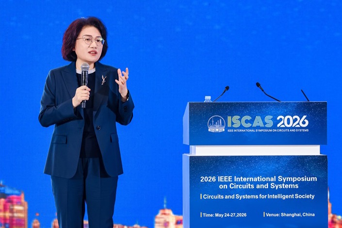
Die USA tun alles, um Chinas Techindustrie auf Abstand zu halten, doch Huawei gibt sich optimistisch: Auf einer Konferenz in Shanghai kündigte das Unternehmen einen Durchbruch in der Halbleiterproduktion an.

Leggi questa versione → originale
siliconangle.com1 g fa

China's Huawei unveils new sanctions-busting chip architecture that replaces Moore's Law - SiliconANGLE

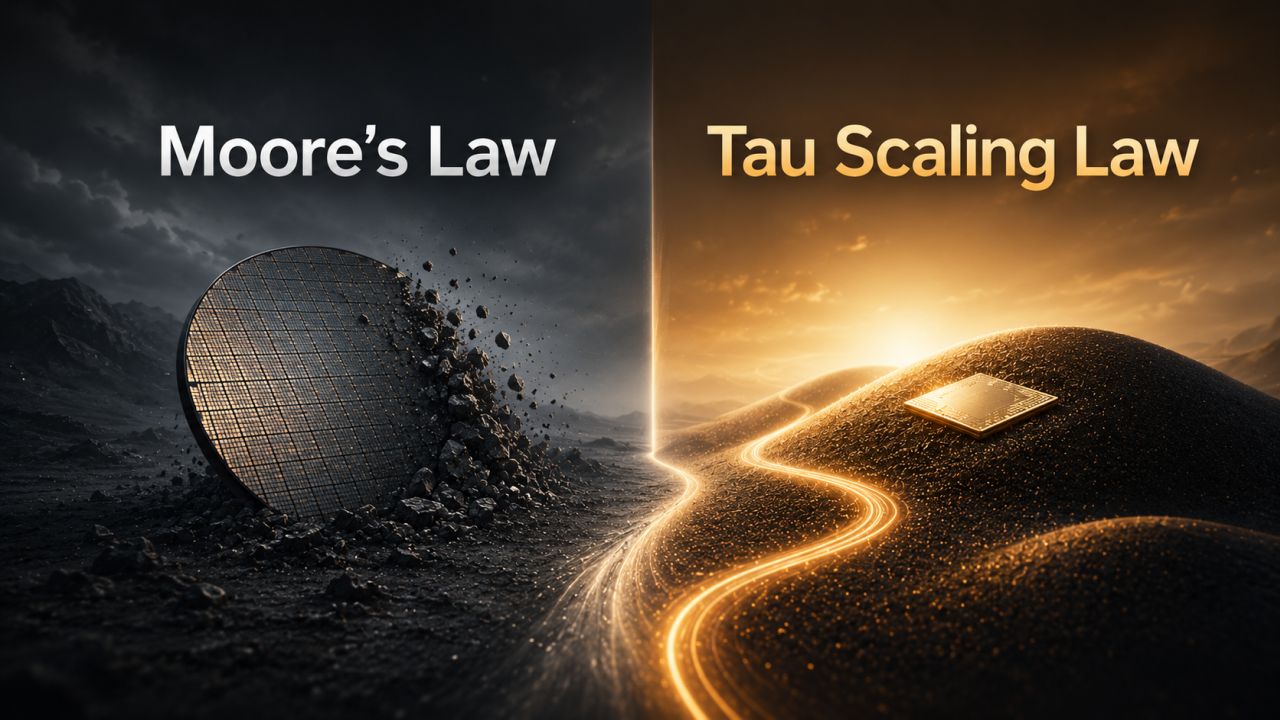
Huawei unveiled LogicFolding, a stacked dual-layer chip architecture based on its proprietary Tau Scaling Law, targeting 55% transistor density gains and 1.4nm-class performance by 2031 — without EUV lithography machines blocked by U.S. sanctions. If the roadmap holds, it gives China a credible domestic alternative to TSMC/Nvidia for AI datacenter silicon, reshaping the assumption that export controls alone can contain Chinese semiconductor advancement.

Leggi questa versione → originale
tomshardware.com1 g fa

Huawei claims sanctions-busting breakthrough with 1.4nm-class chips by 2031, claims 55% higher transistor…

Flagship Huawei Mate 90 series will be the first commercial processors to feature the LogicFolding architecture

Leggi questa versione → originale
dday.it1 g fa

Huawei sfida TSMC e Intel: chip “equivalenti” a 1,4 nm senza litografia avanzata

Non avendo accesso alla litografia avanzata, Huawei si getta nello spazio 3D logico. Con Tau Scaling Law e LogicFolding, promette più densità e meno ritardi nei segnali. Il primo banco di prova sarà il Kirin atteso in…

Leggi questa versione → originale
qz.com10 h fa

Huawei LogicFolding chip design aims to match 1.4nm by 2031

The Chinese tech giant says its new stacked-chip architecture can deliver transistor density equivalent to 1.4nm processes by 2031, without access to advanced lithography tools

Leggi questa versione → originale
  • lunedì 25 maggio 2026·economictimes.indiatimes.com

    Huawei proposes new path for chip development amid US sanctions - The Economic Times

    Huawei aims for advanced chip design by 2031. The company is developing a new 'Tau Scaling Law' to improve chip performance. This innovation could bypass US sanctions restricting…

  • lunedì 25 maggio 2026·thenextweb.com

    Huawei unveils ‘Tau Scaling Law’ as China’s workaround for US chip sanctions

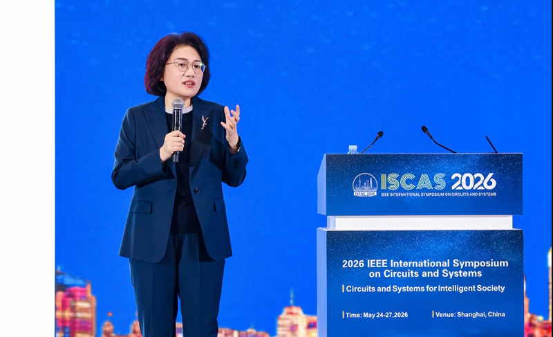
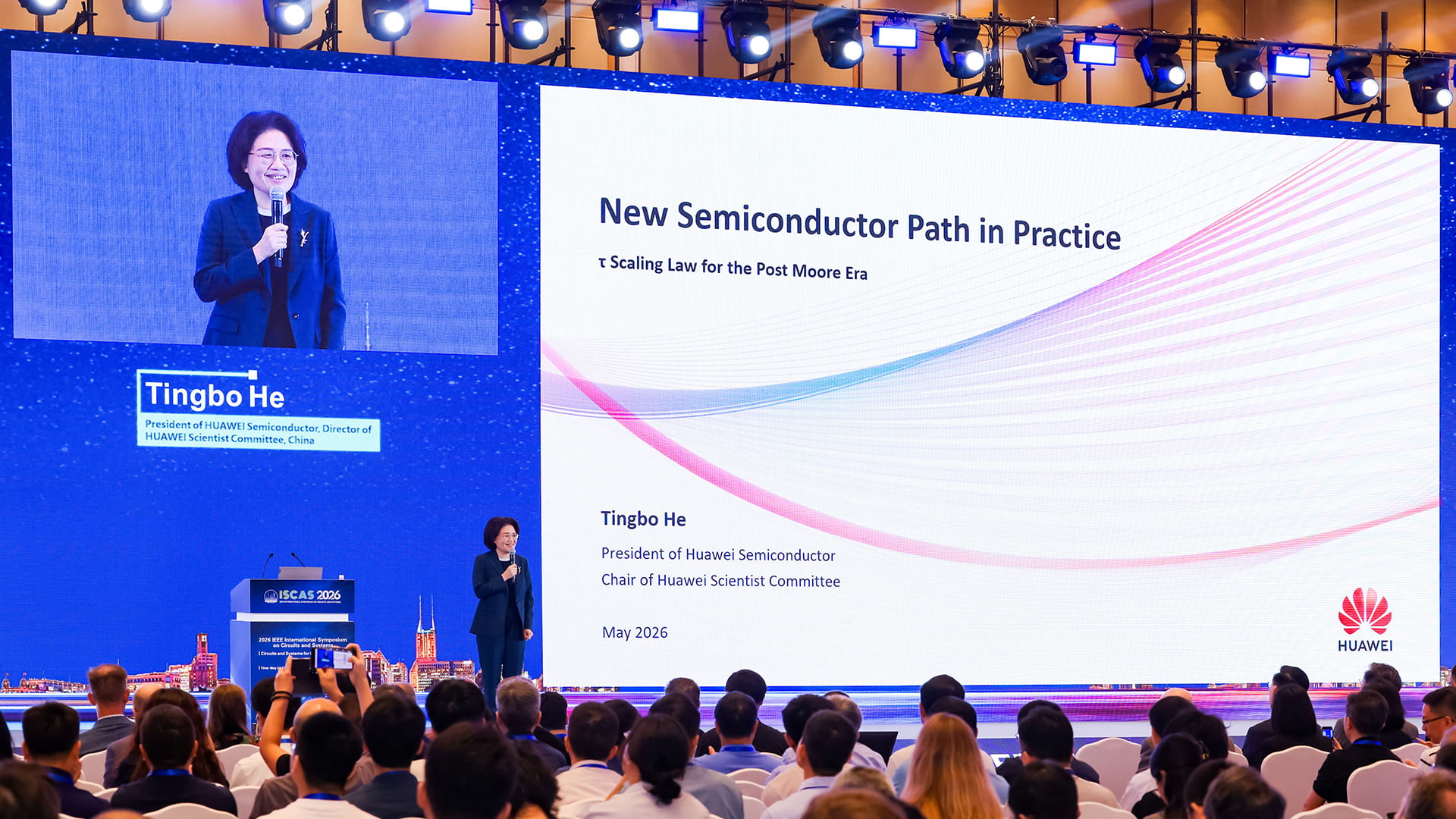
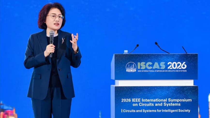
    Huawei's He Tingbo used an ISCAS keynote in Shanghai to pitch the Tau Scaling Law, a chip-design approach built around signal time rather than transistor size.

  • lunedì 25 maggio 2026·malaymail.com

    Huawei unveils chip design breakthrough, targets 1.4‑nm‑equivalent density by 2031 despite US curbs

    Huawei unveils chip design strategy to boost performanceStrategy focuses on scaling, rather than making transistors smallerHuawei expects to design chips by 2031 with density...

  • lunedì 25 maggio 2026·dday.it

    Huawei sfida TSMC e Intel: chip “equivalenti” a 1,4 nm senza litografia avanzata

    Non avendo accesso alla litografia avanzata, Huawei si getta nello spazio 3D logico. Con Tau Scaling Law e LogicFolding, promette più densità e meno ritardi nei segnali. Il primo…

  • lunedì 25 maggio 2026·siliconrepublic.com

    Huawei proposes new path for chips as Moore’s Law runs out of road

    Huawei has proposed a new guiding principle for the semiconductor industry that could allow it to close gap with TSMC.

  • lunedì 25 maggio 2026·hwupgrade.it

    Altro che Legge di Moore, HUAWEI punta sulla Tau Scaling Law per i semiconduttori: di cosa si tratta

    HUAWEI ha presentato la Tau Scaling Law, una nuova legge per l'evoluzione dei semiconduttori alternativa alla tradizionale miniaturizzazione geometrica. L'azienda punta su…

  • lunedì 25 maggio 2026·manager-magazin.de

    Trotz US-Sanktionen: Chinas Huawei kündigt Durchbruch bei Chipentwicklung an

    Die USA tun alles, um Chinas Techindustrie auf Abstand zu halten, doch Huawei gibt sich optimistisch: Auf einer Konferenz in Shanghai kündigte das Unternehmen einen Durchbruch in…

  • lunedì 25 maggio 2026·tomshardware.com

    Huawei claims sanctions-busting breakthrough with 1.4nm-class chips by 2031, claims 55% higher transistor density — firm claims new…

    Flagship Huawei Mate 90 series will be the first commercial processors to feature the LogicFolding architecture

  • martedì 26 maggio 2026·siliconangle.com

    China's Huawei unveils new sanctions-busting chip architecture that replaces Moore's Law - SiliconANGLE

    China's Huawei unveils new sanctions-busting chip architecture that replaces Moore's Law - SiliconANGLE

  • martedì 26 maggio 2026·global.chinadaily.com.cn

    Huawei unveils cutting-edge chip-development framework

    Huawei Technologies Co expects its premium chips to achieve transistor density equivalent to 1.4-nanometer processes by 2031 under a new semiconductor development framework, the…

  • martedì 26 maggio 2026·kr-asia.com

    Huawei proposes “Tau scaling law” to extend chip advances beyond Moore’s law

    The framework could help Huawei’s chips achieve 1.4-nm-equivalent transistor density by 2031.

  • martedì 26 maggio 2026·qz.com

    Huawei LogicFolding chip design aims to match 1.4nm by 2031

    The Chinese tech giant says its new stacked-chip architecture can deliver transistor density equivalent to 1.4nm processes by 2031, without access to advanced lithography tools

  • martedì 26 maggio 2026·theregister.com

    Huawei's chip law looks less like Moore and more like marketing

    Chinese tech biz shows off clever workaround for its process node gap, but it isn't catching up with Intel and TSMC

  • martedì 26 maggio 2026·heise.de

    Chip-Lithografie: Huawei will Moore's Law ablösen

    Huawei hat aufgrund der Sanktionen Schwierigkeiten, Transistoren weiter zu schrumpfen. Kurze Signalwege mit gestapelten Chips sollen die Probleme kaschieren.