The tech giant claims it can reach cutting-edge chip density by 2031, closing the gap with TSMC.
Huawei has proposed a new guiding principle for the semiconductor industry that it says could allow it to design chips rivalling the world’s most advanced processes, without needing the cutting-edge manufacturing equipment it has been denied under US sanctions.
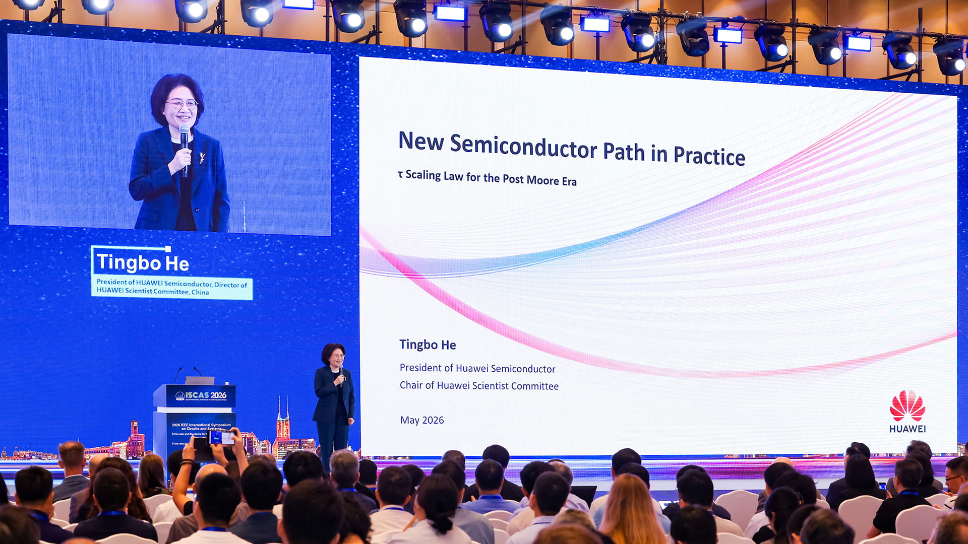
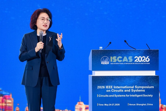
At the 2026 IEEE International Symposium on Circuits and Systems (ISCAS) in Shanghai today (25 May), He Tingbo, president of Huawei’s semiconductor business and chair of its Scientist Committee, delivered a keynote speech entitled ‘New Semiconductor Path in Practice’, in which she presented what the company calls the ‘Tau Scaling Law’.
The law proposes replacing geometric scaling, the decades-old practice of physically shrinking transistors, with time scaling as the new guiding principle for semiconductor evolution. The idea is to reduce the time it takes for signals to propagate through chips and computing systems rather than making individual components smaller.
The principle has already acquired a nickname: “Her’s Law”, according to the South China Morning Post – a play on both He Tingbo’s surname and the tradition of naming foundational scientific laws after their originators, as with Moore’s Law.