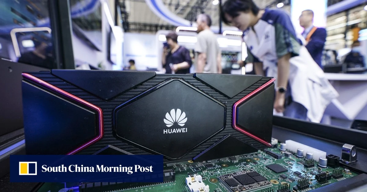
When the US cut Huawei off from the world’s most advanced chipmaking tools in 2019, most industry watchers assumed the Chinese tech giant would hit a ceiling. Instead, Huawei just redefined what a ceiling looks like.
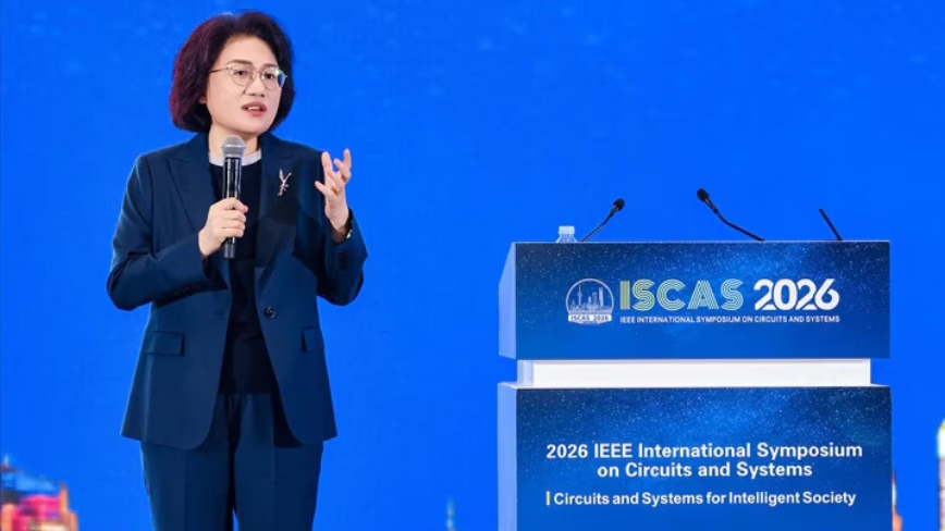
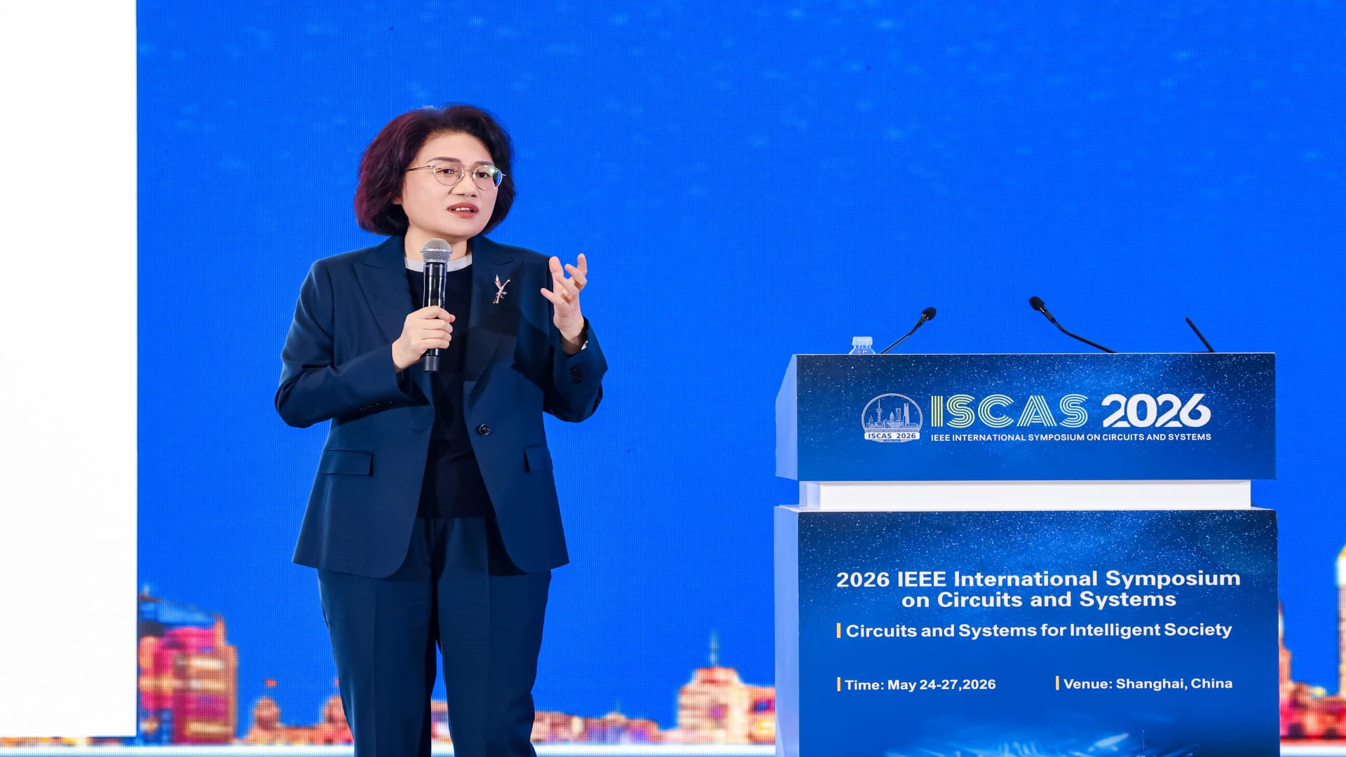
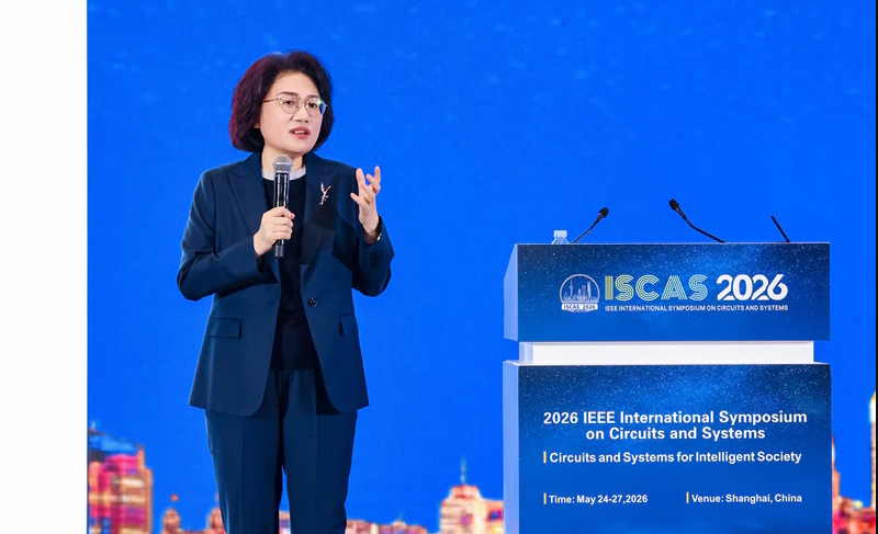
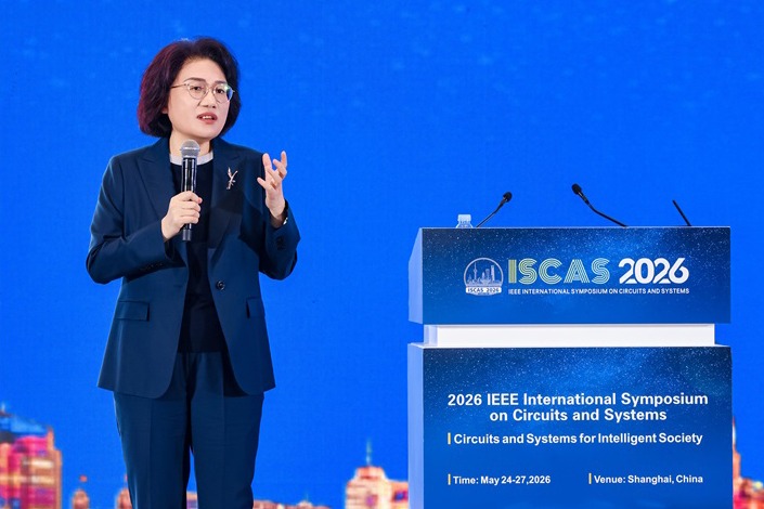
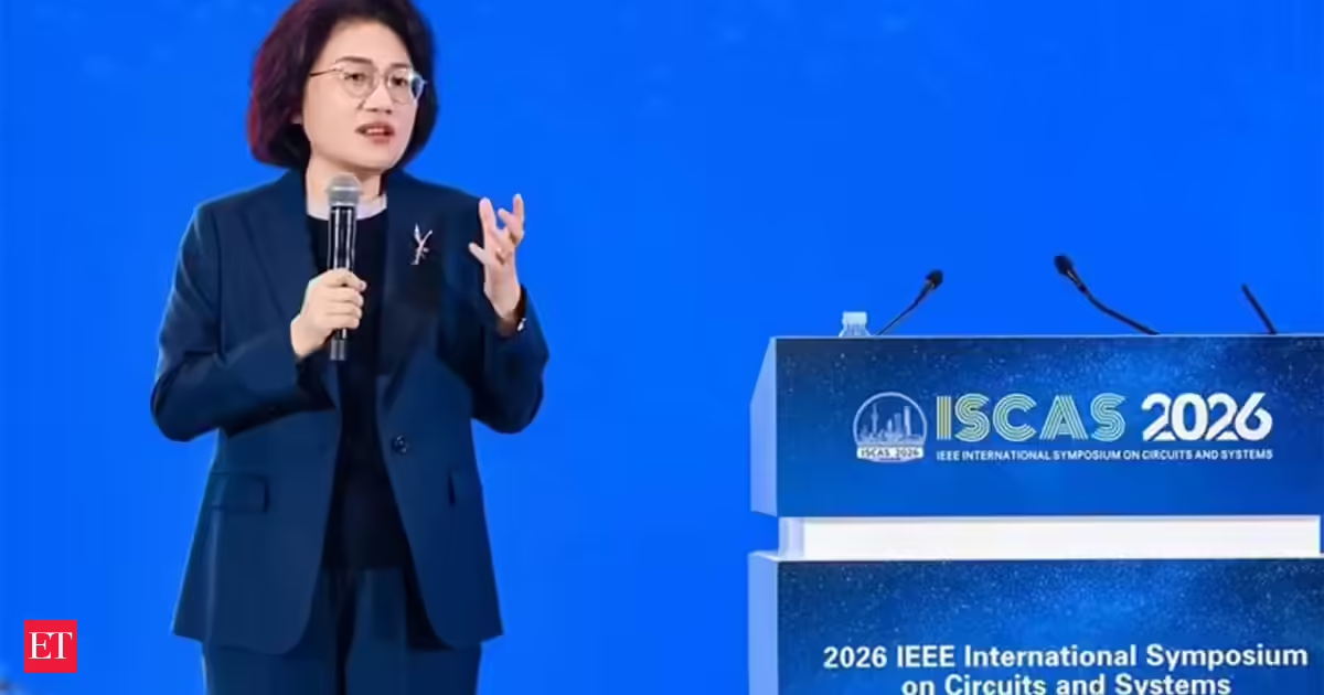
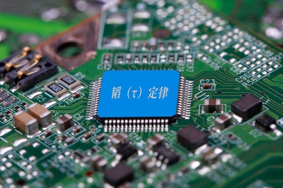
At the IEEE International Symposium on Circuits and Systems (ISCAS 2026) in Shanghai on May 25, He Tingbo, president of Huawei’s semiconductor division, introduced what the company calls the “Tau Scaling Law.” The core idea: stop obsessing over making transistors smaller and start optimizing how fast signals and data actually move through a chip.
A different kind of Moore’s Law successor
Huawei’s new approach flips that script entirely. Rather than geometric scaling, which requires cutting-edge extreme ultraviolet (EUV) lithography machines that US sanctions have placed firmly out of reach, the Tau Scaling Law focuses on reducing latency at the system level.
The technical backbone of this strategy is a new 3D circuit architecture called LogicFolding. He Tingbo projected that the approach could achieve transistor density equivalent to 1.4 nm processes for high-end chips by 2031. That would represent improvements of up to 55% in transistor density and 41% in power efficiency compared to current designs.