China’s Huawei unveils new sanctions-busting chip architecture that replaces Moore’s Law
Chinese electronics giant Huawei Technologies Co. Ltd. today unveiled a new chip design framework that it says will help it to close the gap in the semiconductor industry with global leaders like Taiwan Semiconductor Manufacturing Co. and Nvidia Corp.
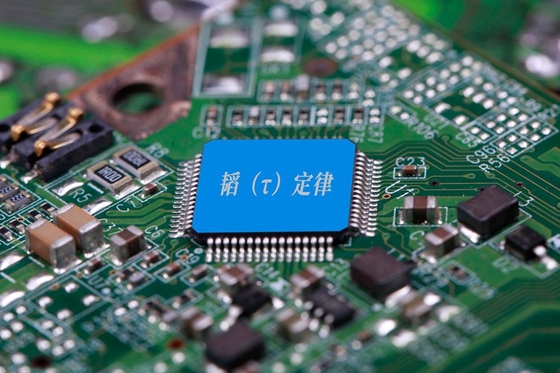
The company also announced a new “Tau Scaling Law” as a replacement for Moore’s Law in future chip scaling, and said it’s targeting 1.4-nanometer class chips and a 55% increase in transistor density by 2031.
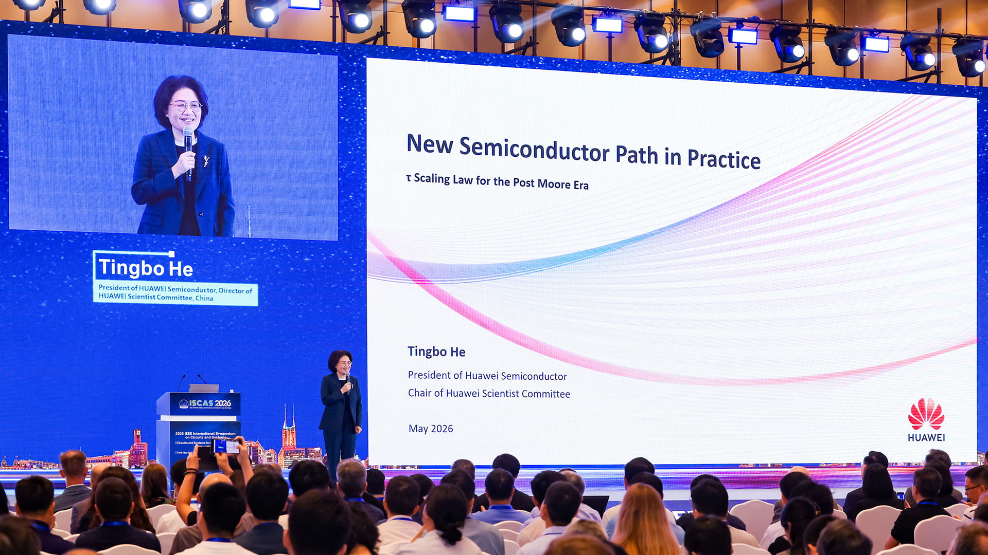
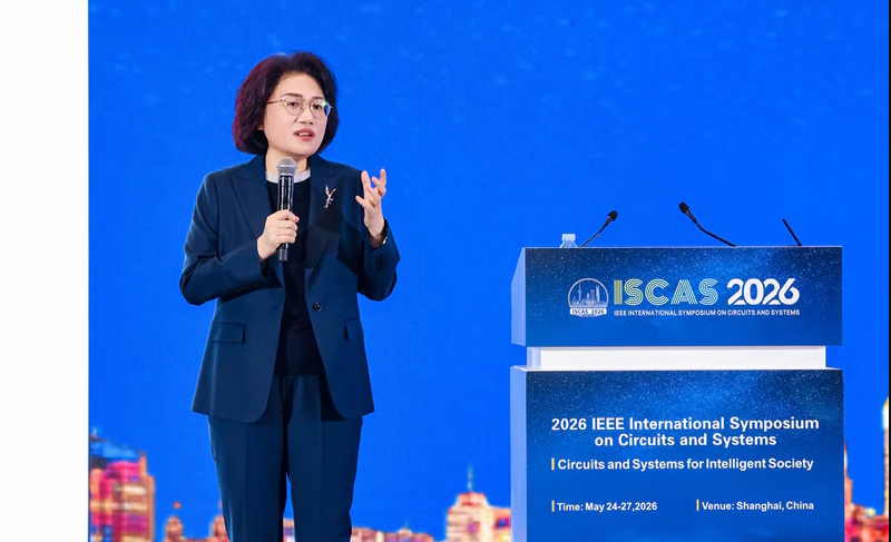
Announced at the Institute of Electrical and Electronics Engineers’ International Symposium on Circuits and Systems in Shanghai today, the new chip design method is primarily about helping China to circumvent the strict sanctions placed on it by the United States. In the last few years, the U.S. has increasingly tightened its restrictions on the kinds of chips China can import from western countries, preventing it from importing the most advanced semiconductors and also the most sophisticated extreme ultraviolet or EUV lithography machines required to manufacture them.
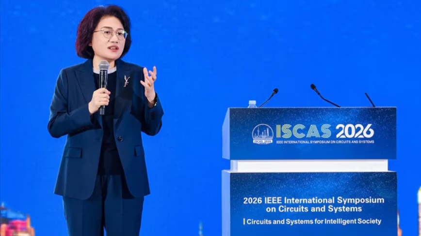
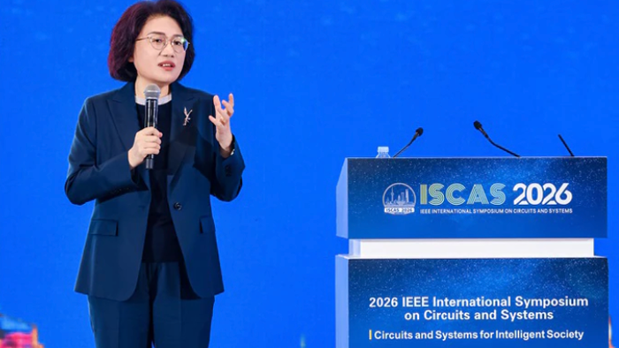
During a keynote address at the event, Huawei’s He Tingbo (pictured), a board member and Chairman of its HiSilicon Semiconductor division, unveiled a new proprietary “LogicFolding” architecture for chip design. It’s a cutting-edge blueprint that’s based on the new Tau Scaling Law. He revealed that Huawei has spent more than six years quietly refining the architecture, which introduces a new methodology for manufacturing advanced processors. During that time, it has secretly designed and produced 381 chips based on the blueprint, validating its engineering principles. The architecture will finally make its commercial debut this autumn with the launch of Huawei’s new flagship Kirin smartphone processor, He said.