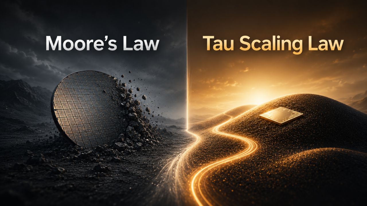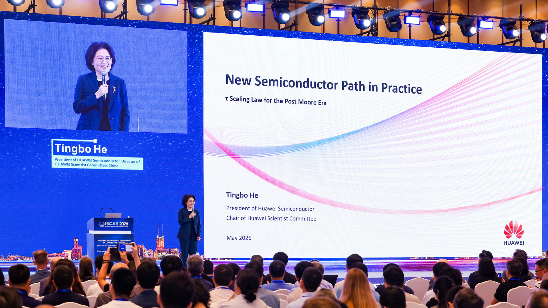
Huawei has proposed a new semiconductor development framework called the “Tau scaling law,” framing it as an alternative method to improve chip performance as Moore’s law becomes harder to sustain.
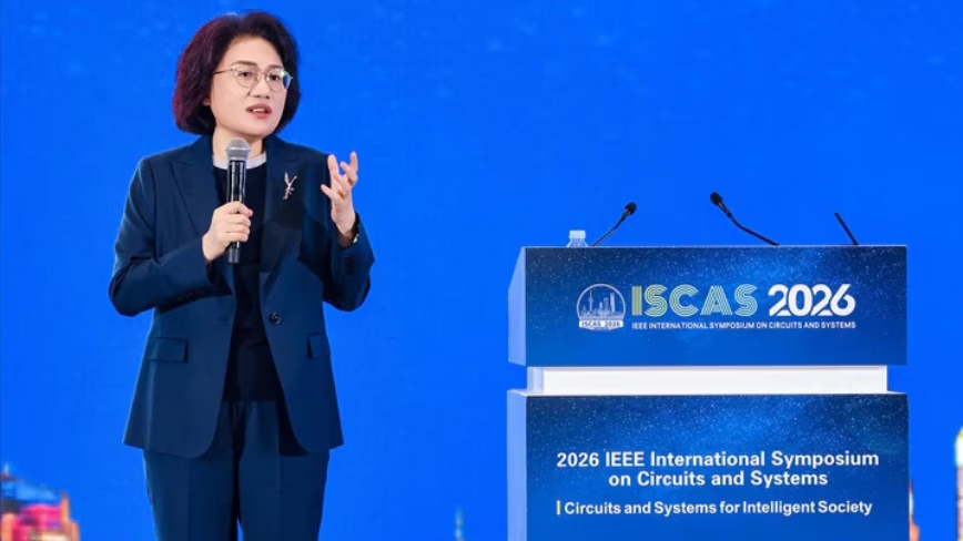
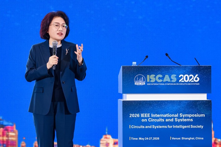
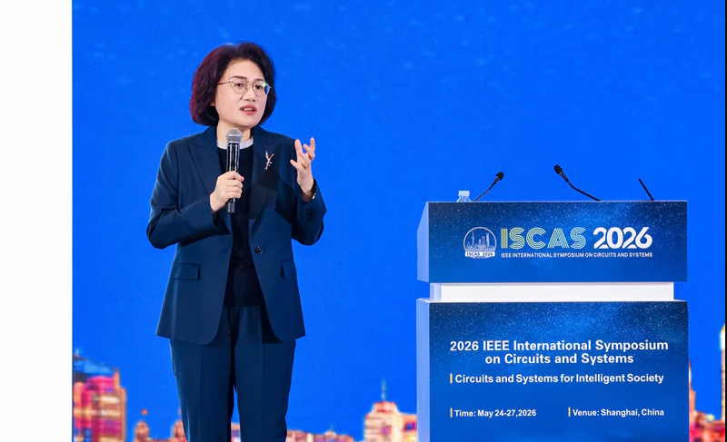
The proposal was introduced on May 25 at the IEEE International Symposium on Circuits and Systems in Shanghai by He Tingbo, chairwoman of Huawei’s scientist committee and president of its semiconductor business department. In her keynote, she described Tau scaling as a shift from geometric scaling, the traditional method of shrinking transistors, to time-based scaling, where chip performance is improved by reducing signal delay across devices, circuits, chips, and systems.
“Losing geometric scaling does not mean losing time scaling,” He said.
She added that one core technology under this approach is LogicFolding, an architecture designed to shorten critical wiring paths, reduce signal propagation delay, and improve transistor density and circuit performance. The company said Kirin chips scheduled for launch in fall and winter 2026 will be the first to adopt LogicFolding.
Dubbed “Her’s law” by He’s peers, Tau scaling is less about shrinking the chip, as Moore’s law is, and more about shortening the journey inside it. By shifting the emphasis to architecture and signal efficiency, the approach could reduce dependence on the most advanced lithography tools, though not eliminate it.