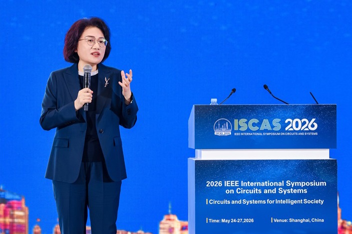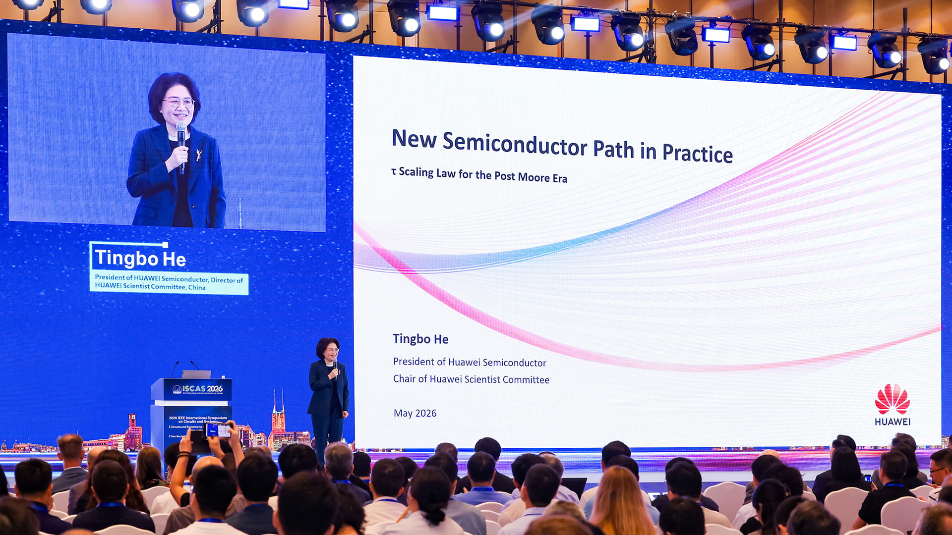
Huawei Technologies has unveiled a new scaling law and chip architecture that can bring its chips equivalent to a process node of 1.4 nanometre by 2031, in a key step by the Chinese tech giant to establish a self-reliant semiconductor ecosystem.The company claims the new Tau (τ) Scaling Law, which was presented by He Tingbo, chair of Huawei Scientist Committee and president of the company’s semiconductor business department on Monday, is a new principle that guided “evolution of both semiconductors and electronic systems”.During He’s keynote speech delivered at the 2026 IEEE International Symposium on Circuits and Systems (ISCAS) in Shanghai on Monday, she said Huawei had been using the new scaling law to design and mass produce 381 chips over the past six years.Also dubbed “Her’s Law” by He’s peers, the new principle proposes a paradigm shift that replaced the traditional geometric miniaturisation of transistors with time (τ) scaling.Based on the law, He also unveiled an innovative core technology called LogicFolding architecture, which can reduce the resistive and capacitive load of signal propagation, ultimately boosting transistor density.The company expects its self-developed high-end chips, based on the new scaling law, to feature a transistor density equivalent to 1.4 nm processes by 2031. Its new Kirin chips, which are scheduled to launch later this year, will be the first to adopt the LogicFolding architecture with enhanced chip performance, He added.
Huawei unveils new scaling law and tech that can develop 1.4 nm equivalent chips
The Chinese tech giant’s new breakthrough is a major milestone in its mission to create a self-reliant semiconductor ecosystem.
228 words~1 min read