TL;DRHuawei’s semiconductor chief He Tingbo returned to public life after seven years to unveil the Tau Scaling Law and LogicFolding architecture. The company claims it can reach 1.4nm-equivalent chip density by 2031 without EUV lithography, but faces steep hurdles in heat dissipation, EDA tooling, and yield rates.
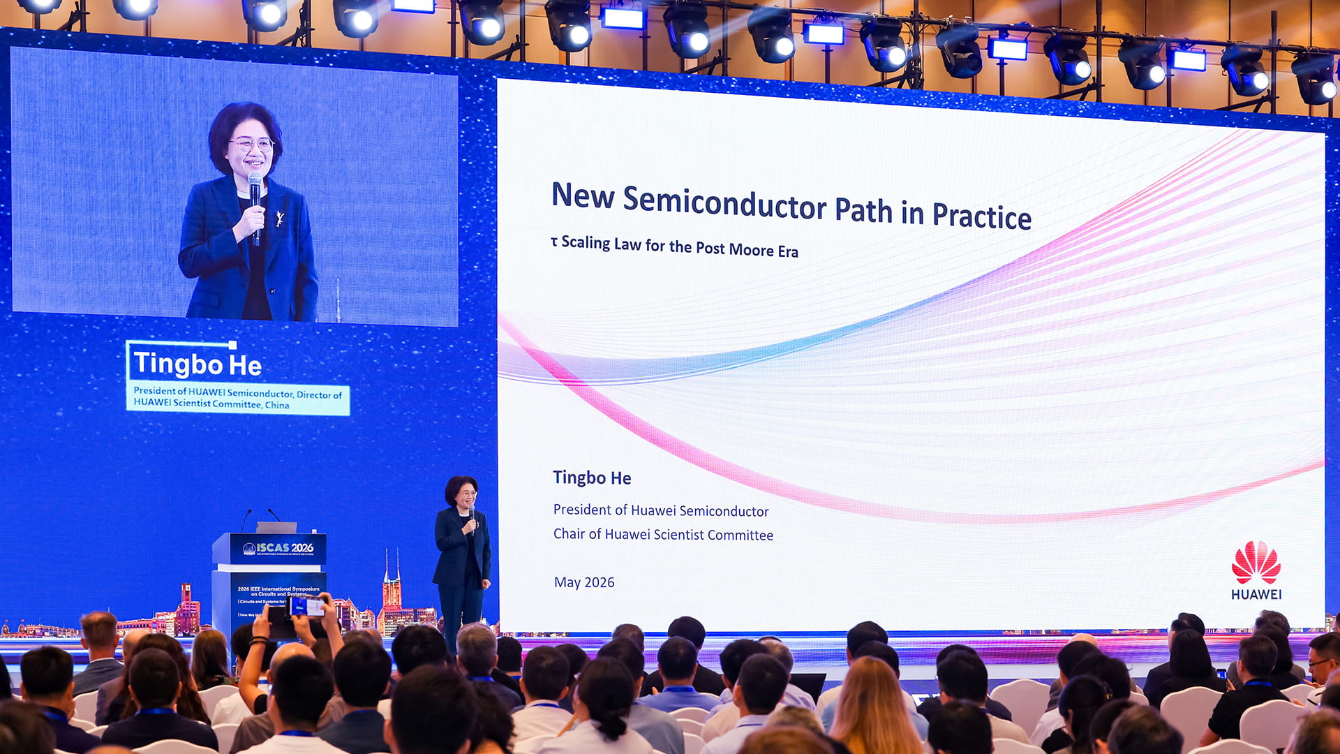
For seven years, He Tingbo worked in silence. The head of Huawei’s semiconductor business, widely known as the company’s “chip queen,” vanished from public view in 2019 after Washington severed the Chinese company’s access to advanced technology.
Her retreat became a symbol of Huawei’s fight for survival. That changed on 25 May at the IEEE International Symposium on Circuits and Systems in Shanghai, where she delivered a keynote titled “New Semiconductor Path in Practice.”
A new law for a new era
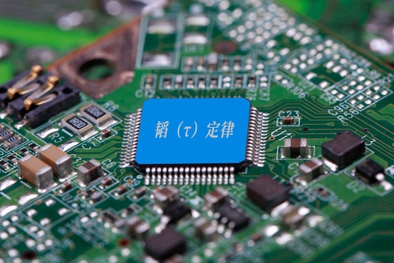
He introduced the “Tau (τ) Scaling Law,” a principle that replaces geometric transistor shrinking with signal-propagation time as the metric of progress. Named after the Greek letter for propagation delay, the law focuses on compressing signal travel time across devices and circuits rather than making transistors physically smaller.