Huawei just told the world it plans to close a five-year technology gap with the most important chipmaker on the planet.
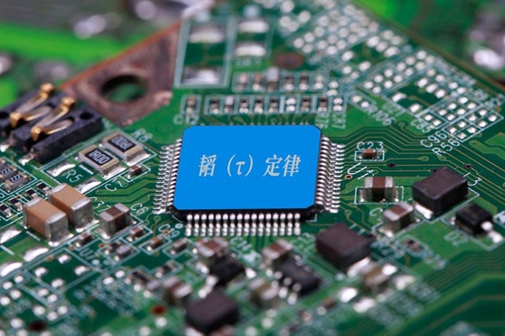
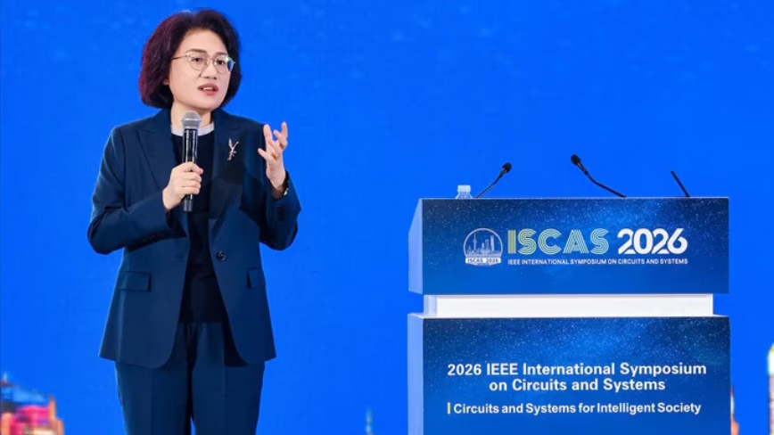
At the IEEE International Symposium on Circuits and Systems (ISCAS) in Shanghai, Huawei unveiled what it calls the Tau Scaling Law and a companion technology called LogicFolding. Together, these proprietary methods aim to achieve transistor density and performance equivalent to 1.4-nanometer chips by 2031. For context, TSMC is targeting mass production of actual 1.4nm chips by 2028. So Huawei is essentially saying: give us three extra years, and we’ll get to the same destination using a completely different road.
The EUV problem, and Huawei’s detour around it
The gold standard process requires extreme ultraviolet (EUV) lithography machines, which are manufactured by ASML in the Netherlands. These machines cost hundreds of millions of dollars each and are the bottleneck through which all advanced chipmaking must pass. Thanks to US export controls, Chinese firms like Huawei and its foundry partner SMIC cannot buy them.
The Tau Scaling Law and LogicFolding represent an attempt to achieve comparable transistor density without EUV lithography. Rather than shrinking transistors the traditional way, which requires increasingly precise light wavelengths to etch smaller and smaller features, Huawei is exploring architectural innovations that stack and fold logic in ways that approximate the density gains of smaller process nodes.