Bloomberg / Getty Images
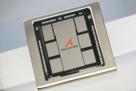
Huawei unveiled a chip architecture on Monday that folds traditional flat circuits into vertical, stacked structures, which the company says will allow it to produce chips with transistor density equivalent to 1.4-nanometer processes by 2031 — without relying on advanced manufacturing equipment it cannot access under U.S. sanctions.
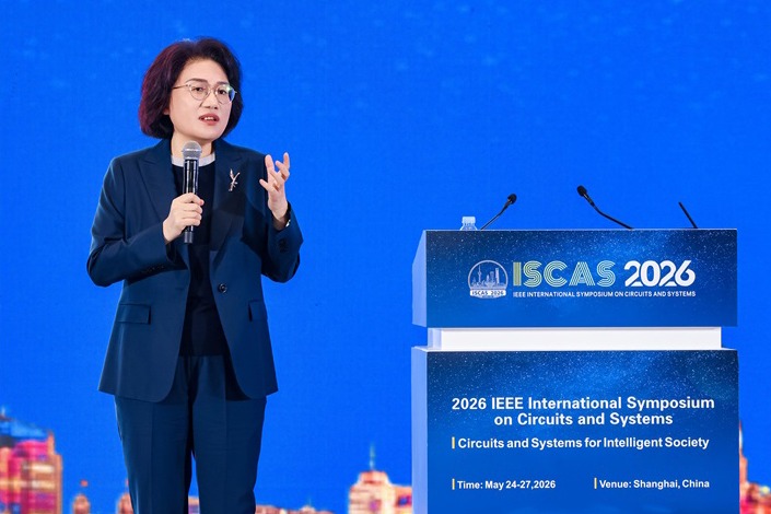
He Tingbo, president of Huawei's semiconductor business, presented the approach at the IEEE International Symposium on Circuits and Systems in Shanghai. The technique, called LogicFolding, shortens the wiring inside chips by expanding circuit layouts from one layer to two, which the company said reduces signal travel time and raises transistor density.
Huawei paired the announcement with a new guiding principle it calls the Tau Scaling Law, which replaces the traditional goal of shrinking transistors — the basis of Moore's Law — with a focus on cutting the time it takes signals and data to move through chips and computing systems.
To appreciate the ambition behind that figure, it helps to know that 7nm represents roughly the ceiling of what China's domestic chipmakers have been able to reliably demonstrate, according to Reuters. For comparison, TSMC $TSM -0.65% — the Taiwan-based foundry that sits at the top of the global chip industry — is already running volume production at 2nm and has a 1.4nm process slated for mass production in 2028, according to NBC News.