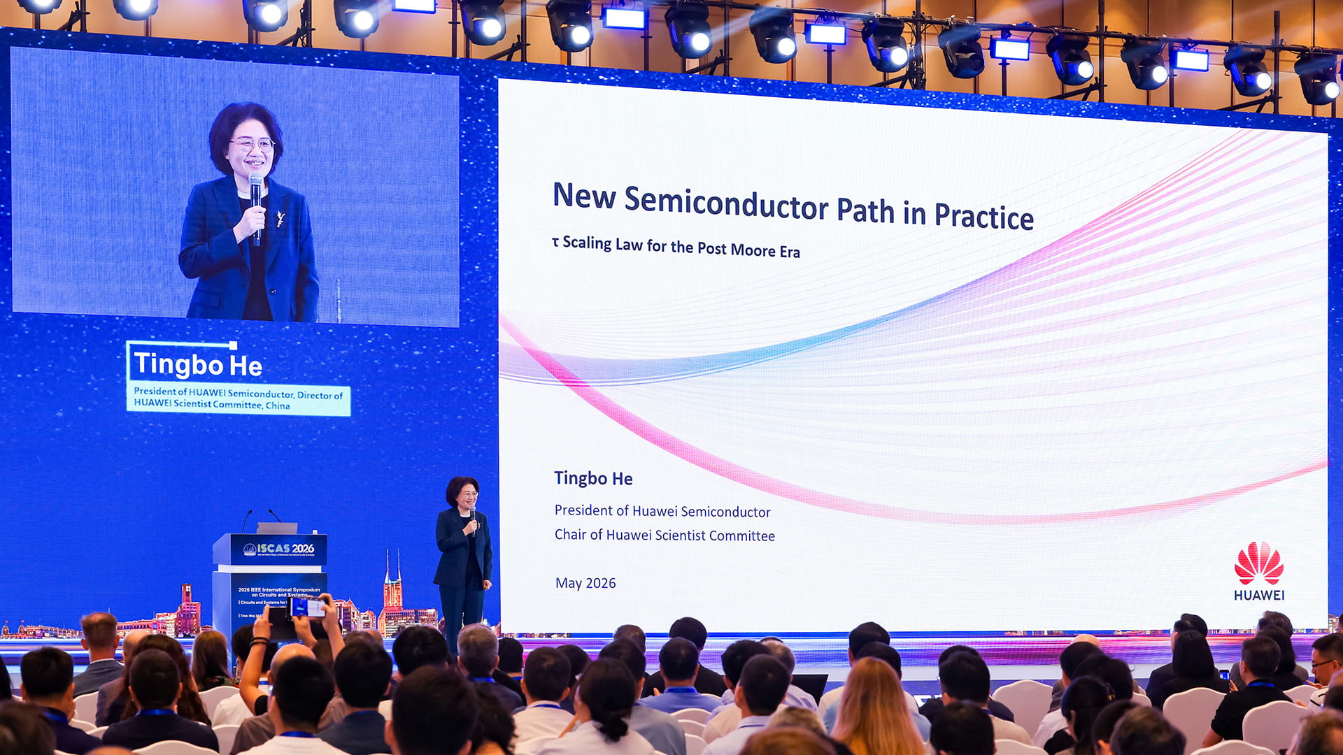
Huawei Technologies Co expects its premium chips to achieve transistor density equivalent to 1.4-nanometer processes by 2031 under a new semiconductor development framework, the company announced on Monday at a conference in Shanghai.
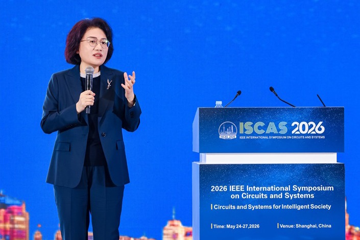
He Tingbo, Huawei board member and president of its semiconductor business, formally introduced the "Tau Scaling Law" in a keynote speech titled "New Semiconductor Path in Practice."
Unlike traditional approaches that rely on miniaturizing transistors — an industry paradigm increasingly challenged by physical limits and diminishing cost benefits — the new methodology prioritizes reducing signal propagation time across devices, circuits, chips and systems, He said.
Huawei has already designed and mass-produced 381 chips based on the Tau Scaling Law over the past six years, covering industries from smartphones to AI computing, He said.
This autumn, the company will launch a new Kirin smartphone chip that adopts a multi‑layer circuit architecture that shortens critical‑path wiring and improves transistor density and energy efficiency for the first time.