WHAT WE KNOW SO FAR: Huawei Technologies is betting it can sidestep one of the semiconductor industry's most entrenched dependencies: the need for cutting-edge lithography machines. The company says it has developed a way to build advanced chips without access to the specialized equipment that has long defined the global pecking order in chipmaking.
The approach, still in development, aims to produce processors that reach transistor densities comparable to a 1.4-nanometer process by 2031. That level of density is widely viewed as the next milestone for leading chipmakers such as Intel, TSMC, and Samsung Electronics, all of which rely on extreme ultraviolet lithography systems made by ASML.
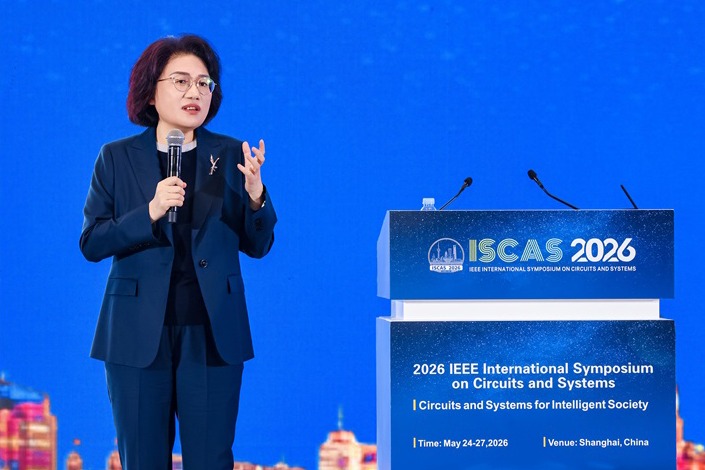
Huawei, which has been blocked from accessing that equipment under US export controls, is instead focusing on redesigning how chips are built internally. "Our solution is feasible and affordable," He Tingbo, president of Huawei's chip arm, said Monday at an event in Shanghai.
Huawei is trying to work around traditional fabrication limits and focusing on architectural changes. Its method centers on stacking multiple layers of circuitry on a single chip and improving the way data moves between them. The goal is to improve performance through efficiency gains rather than further shrinking components.