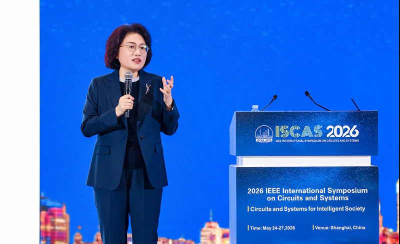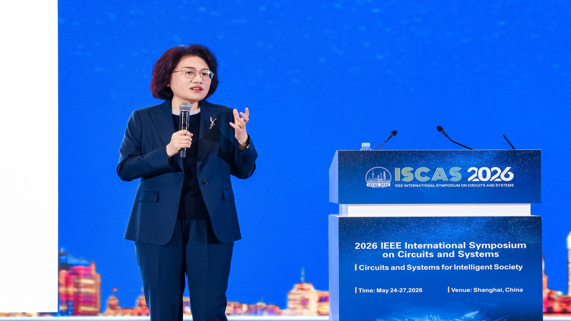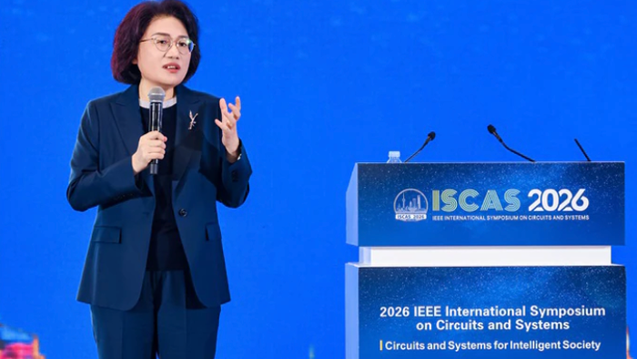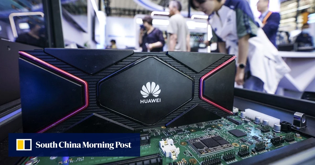
Huawei Technologies’ unveiling of a chip architectural workaround to bypass US sanctions marks a major step towards China’s semiconductor self-sufficiency, giving Beijing powerful new leverage in its tech tug of war with Washington, analysts say.The Chinese tech giant captured global attention on Monday by introducing the new Tau (τ) Scaling Law, which it said lay the groundwork for Huawei to achieve transistor density equivalent to a 1.4-nanometre process in high-end chips by 2031. If proven, the advancement would significantly narrow the gap with global semiconductor leaders at the cutting edge of chip development.“The US will have less leverage over export control as China becomes more self-sufficient,” said Gary Ng, senior economist at Natixis Corporate and Investment Bank, although he cautioned that the law still needed to be “tested in practice”.US-led sanctions currently block China’s semiconductor industry from accessing the most advanced chipmaking technologies, notably extreme ultraviolet (EUV) lithography machines needed for 3nm nodes and below.Huawei’s new trajectory promises to bypass this critical bottleneck. He Tingbo, chairwoman of the Huawei Scientist Committee and president of its semiconductor business department, said cutting-edge EUV tools would no longer be necessary to achieve these advanced nodes.
Huawei breakthrough chips away at Nvidia’s hold on China’s market, analysts say
Chip advance marks big step accelerating China’s semiconductor self-reliance push and promises leaps in AI computing power.
192 words~1 min read