Huawei Technologies said on May 25 it has found a new way to design chips to bring its semiconductor capabilities close to those of global chipmakers Taiwan Semiconductor Manufacturing Company (TSMC) and Intel, as China’s tech champion continues working to overcome US sanctions that have cut it off from top-tier global suppliers.
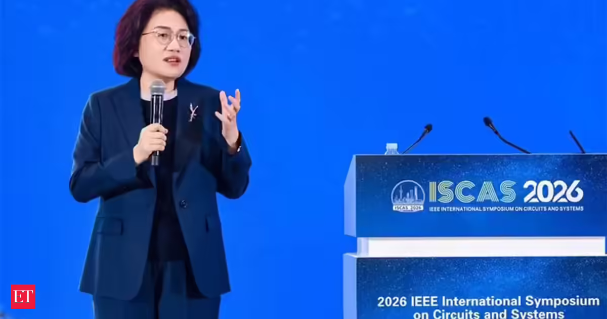
Huawei said that over the past six years, it has developed a new principle, known as the Tau scaling law, to break through the limits of Moore’s Law and keep pursuing advanced semiconductor manufacturing technologies, He Tingbo, Huawei’s semiconductor chief, said at the 2026 IEEE International Symposium on Circuits and Systems, or ISCAS, in Shanghai.
The Tau scaling law is also called “Her’s law” by Huawei, in recognition of He, who joined the company in 1996 and has been leading Huawei’s efforts to develop alternative ways to design chips amid Washington’s persistent crackdown. As president of its semiconductor business department, she has overseen the transformation of chip arm HiSilicon Technologies from a small design team into a globally recognized designer of chips for smartphones, PCs, artificial intelligence computing, and more.
Based on this new principle, He said, engineers can reduce signal delay and steadily improve transistor density to keep advancing chip computing power beyond the limits of Moore’s law, which relies on shrinking transistors ever smaller to increase computing power.