HomeAI · summaries
Storia in 18 fonti
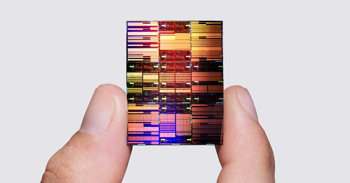
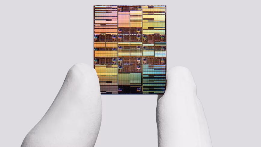
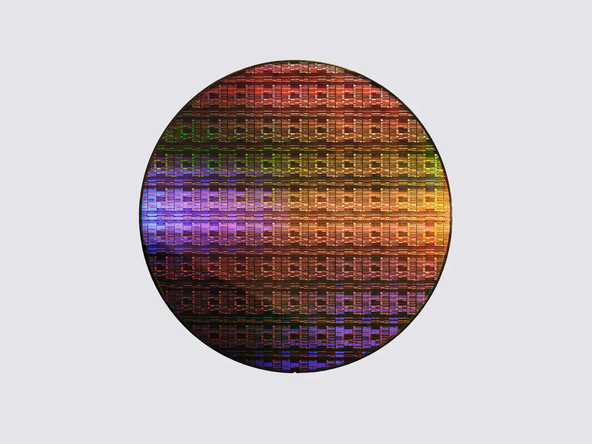
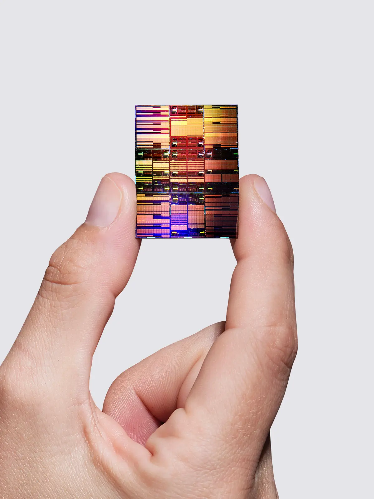
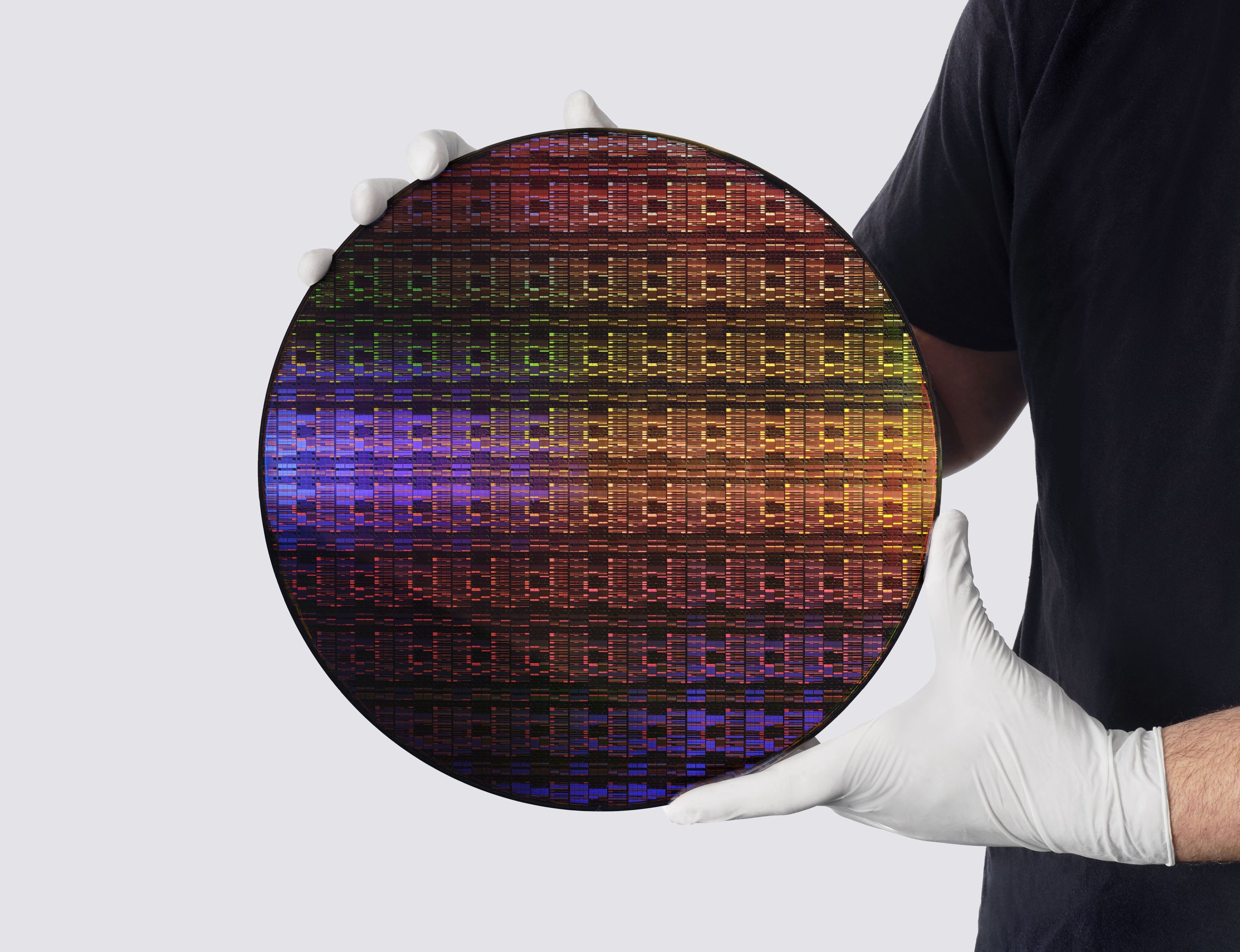
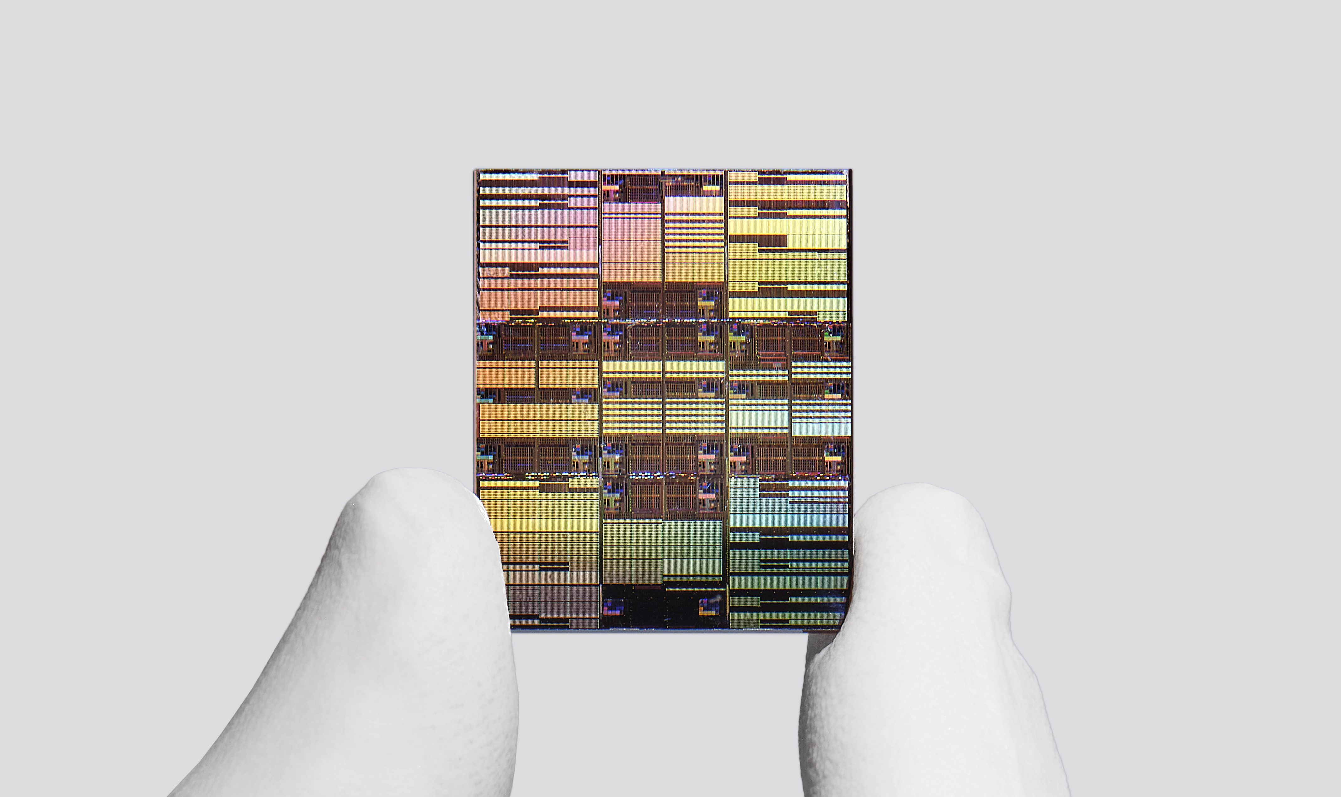
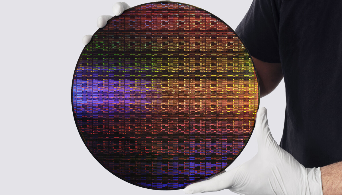
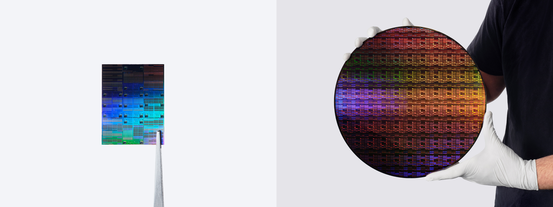
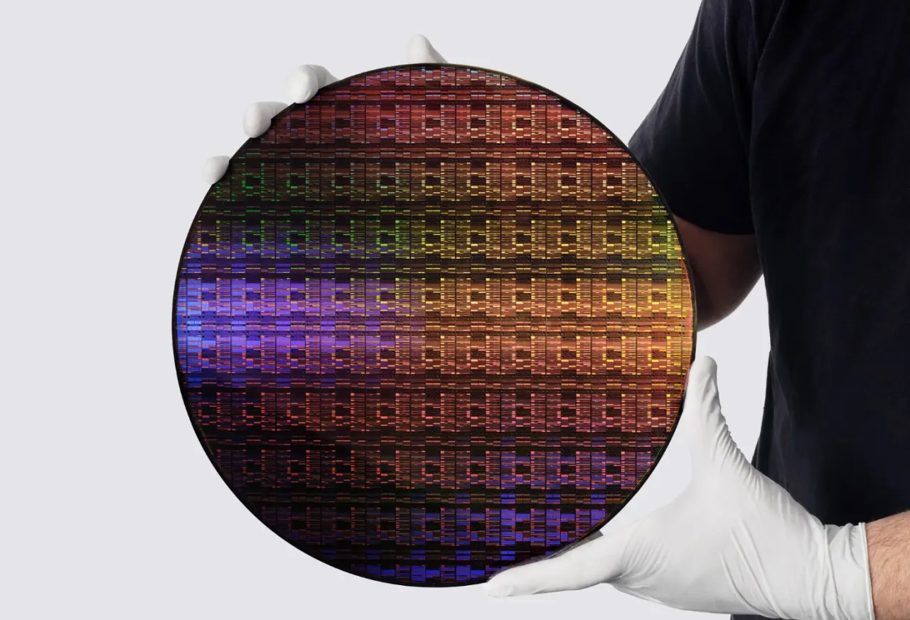
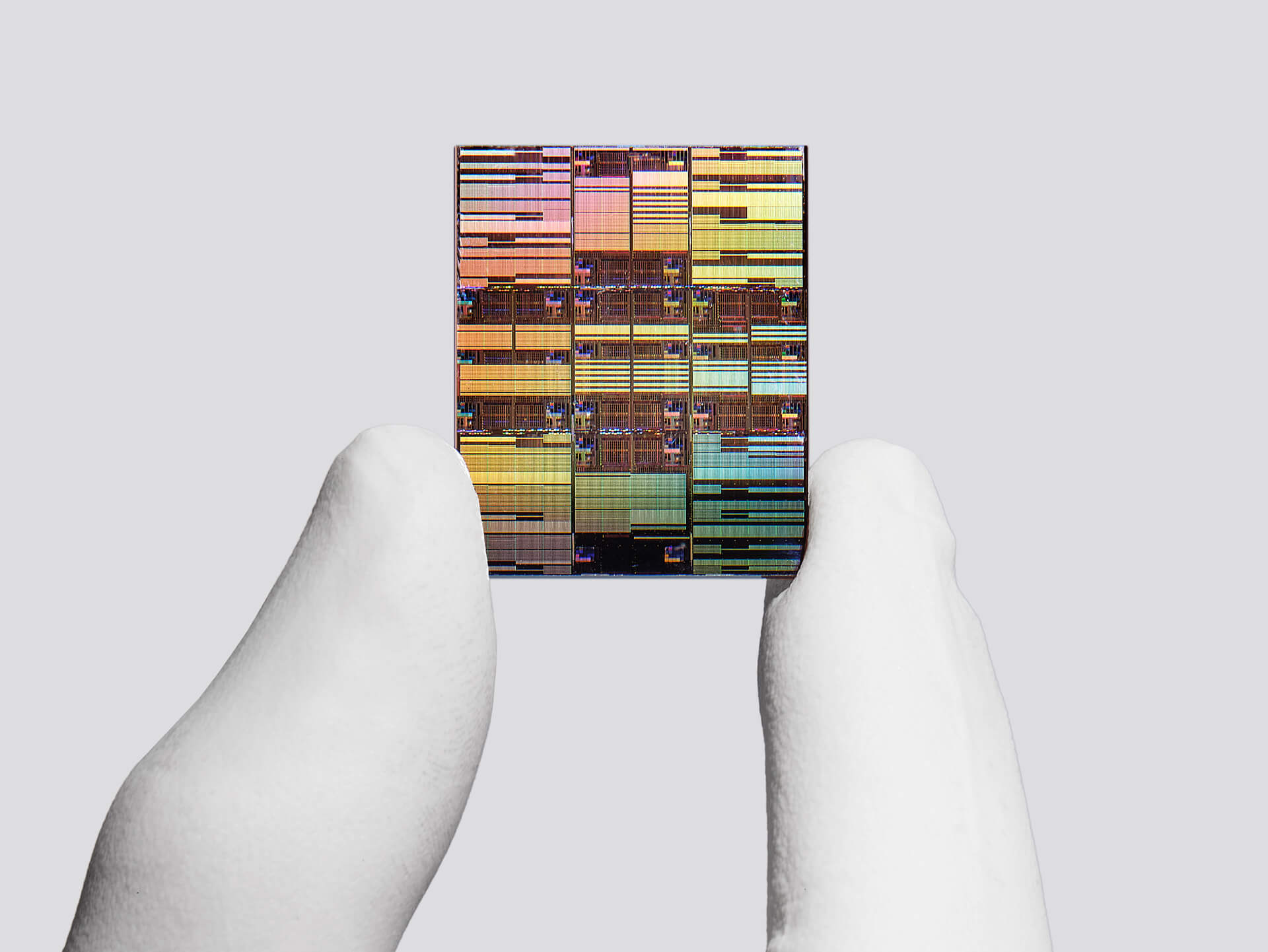
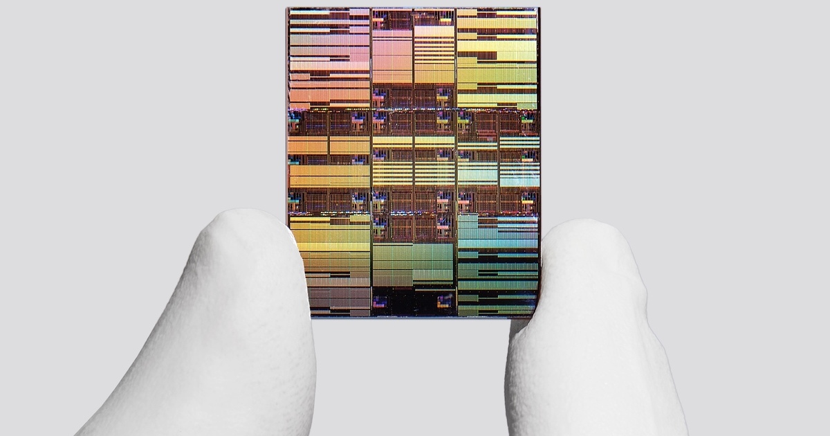
IBM annuncia il primo chip al mondo su nodo a “0,7 nm”
IBM ha annunciato oggi lo sviluppo del primo nodo a 0,7 nanometri o 7 angstrom. Il processo è basato su un’architettura tridimensionale chiamata nanostack, definito come il primo design tridimensionale a nanosheet del settore, con strutture che si avvicinano alla scala atomica
Confronto fonti
6 prospettive sulla stessa storiaTimeline cronologica
- ·
datacenterdynamics.com
IBM details major chip breakthrough with new sub-1nm ‘nanostack’ 3D architecture
Company claims technology provides up to 50 percent more performance or 70 percent greater energy efficiency
- ·
forbes.com

IBM Unveils World’s First Sub-1nm Chip With 100 Billion 3D-Stacked Transistors
IBM just unveiled the world's first sub 1-nanometer chip: 100 billion transistors. IBM also says they've produced functioning devices with this technology.
- ·
thenextweb.com
IBM says it has built the first sub-1nm chip technology
IBM unveiled a 0.7nm chip built on a new 3D ‘nanostack’ architecture, packing nearly 100 billion transistors onto a fingernail-sized chip.
- ·
research.ibm.com
What is IBM’s nanostack chip architecture?
This new microchip architecture from IBM builds up, not out, to overcome the spatial limitations of scaling transistor density.
- ·
IBM introduces the smallest computer chip in the world
It’s the world’s first sub-1nm chip technology, powered by IBM’s new nanostack architecture, paving the way for more powerful chips for years to come.
- ·
g1.globo.com
IBM anuncia primeiro chip do mundo abaixo de 1 nanômetro; entenda o que isso significa | G1
Segundo a empresa, será possível reunir 100 bilhões de transistores em um chip do tamanho de uma unha e aumentar capacidade de desempenho em relação a modelos anteriores.
- ·
siliconangle.com
IBM says new sub-nanometer architecture paves the way for the next decade of chip design - SiliconANGLE
IBM says new sub-nanometer architecture paves the way for the next decade of chip design - SiliconANGLE
- ·
zdnet.com
IBM says it can fit nearly 100 billion transistors on a chip - why the milestone matters
The race for the first sub-one-nanometer chip is over, and IBM has won.
- ·
arstechnica.com
IBM claims world’s first sub-1 nanometer chip technology
IBM’s nanostack transistors could boost chip performance or energy efficiency.
- ·
theregister.com
IBM stacks up a sub-nanometer chip future
Big Blue shows off process node it claims can scale down to 1 Angstrom
- ·
newsroom.ibm.com
IBM Debuts World’s First Sub-1 Nanometer Chip Technology
IBM unveiled a major semiconductor breakthrough with the introduction of the world’s first sub-1 nanometer (nm) chip technology, featuring a revolutionary transistor architecture…
- ·
thehindubusinessline.com

IBM unveils tech for chip smaller than 1 nanometer in AI computing push
IBM introduces groundbreaking 0.7-nanometer chip technology, enhancing AI computing with unprecedented transistor density and efficiency.
- ·
cryptobriefing.com

IBM proposes NanoStack architecture for ultra-dense 3D chips
IBM's NanoStack architecture promises 50% area scaling and 70% power reduction versus 2 nm chips, targeting next-gen AI accelerators and high-performance
- ·
economictimes.indiatimes.com

IBM unveils tech for chip smaller than 1 nanometer in AI computing push - The Economic Times
IBM has unveiled groundbreaking chip technology capable of producing transistors at 0.7 nanometers, a significant leap towards smaller and more powerful semiconductors. This…
- ·
IBM unveils world's first 0.7nm chip technology with 100 billion transistors
IBM unveiled 0.7nm chip technology with 100 billion transistors using nanostack 3D architecture, projecting 50% more performance or 70% better energy
- ·
newsbytesapp.com
IBM reveals world's first sub-1 nanometer chip technology
IBM has introduced groundbreaking technology to produce chips smaller than one nanometer, advancing semiconductor capabilities to meet the rising demands of AI-driven computing.
- ·
neowin.net
IBM reveals sub-1nm chip technology, production expected in another 5 years
IBM has just announced a massive breakthrough in semiconductor research: the world's first sub-1-nanometer chip technology.
- ·
hwupgrade.it

IBM presenta il primo chip al mondo sotto il nanometro: sfiorati i 100 miliardi di transistor
IBM ha presentato il primo chip al mondo sotto il nanometro, con architettura a 0,7 nm e quasi 100 miliardi di transistor: fino al 70% di efficienza in pi� rispetto al nodo a 2 nm…
- ·
ai4business.it
IBM presenta il primo chip sotto 1 nm Nanostack - AI4Business
IBM annuncia un chip sotto 1 nm (0,7 nm) con architettura Nanostack: più densità, meno consumi e nuove prospettive per AI e cloud
- ·
dday.it
IBM annuncia il primo chip al mondo su nodo a “0,7 nm”
IBM ha annunciato oggi lo sviluppo del primo nodo a 0,7 nanometri o 7 angstrom. Il processo è basato su un’architettura tridimensionale chiamata nanostack, definito come il primo…