IBM says new sub-nanometer architecture paves the way for the next decade of chip design
IBM Corp. today unveiled what it says is the world’s first sub-one-nanometer chip technology, a research breakthrough that it said will fuel the next 10 years of semiconductor development and pave the way to atomic-level chip design.
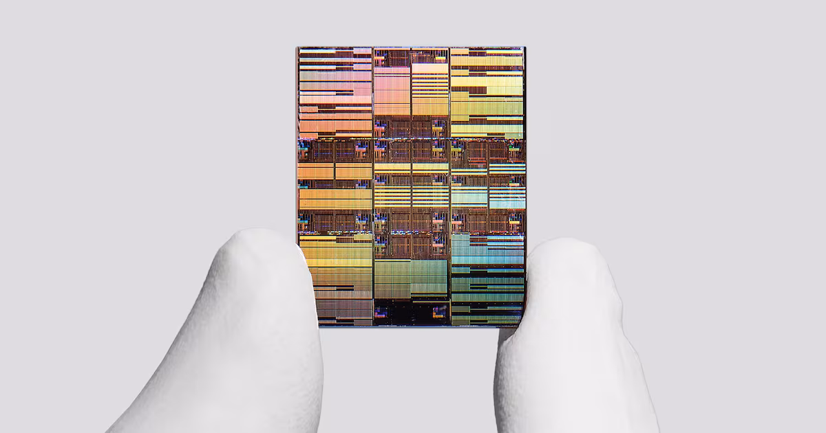
The new technology is based on a transistor architecture IBM calls nanostack, designed for the 0.7-nanometer, or seven-angstrom, node. IBM said the architecture can pack nearly 100 billion transistors onto a chip about the size of a fingernail (pictured), or nearly twice the density of the two-nanometer chip technology the company introduced in 2021.
IBM said the technology is projected to deliver up to 50% better performance and 70% greater energy efficiency compared with its two-nanometer node chips. The company also cited a 40% improvement in static random-access memory scaling, a development it said could be significant for artificial intelligence systems that need high-bandwidth, high-efficiency memory close to compute resources.
“It’s not just an incremental step, it’s a meaningful leap forward… pointing to a future where computing becomes significantly more powerful without a corresponding increase in energy,” said Jay Gambetta, director of IBM Research and an IBM Fellow.