Built with revolutionary “nanostack” 3D chip architecture, IBM’s sub-1 nm chip to propel semiconductor industry forward for the next decade
Jun 25, 2026
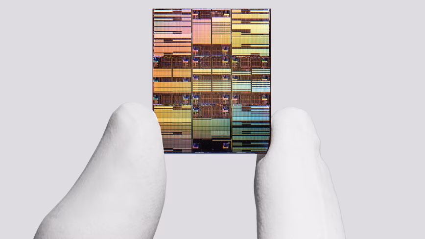
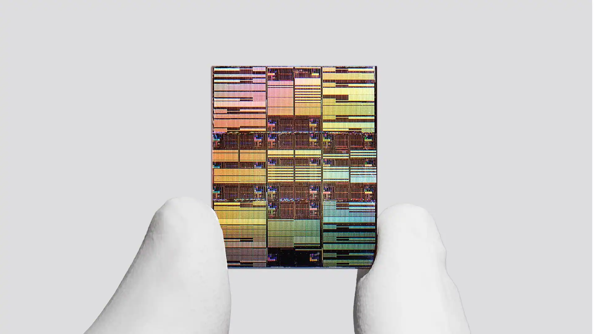
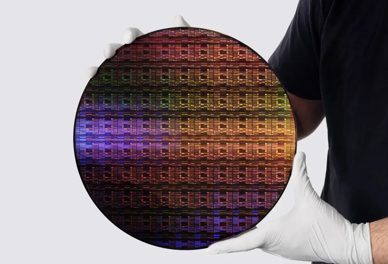
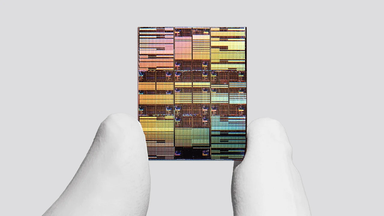
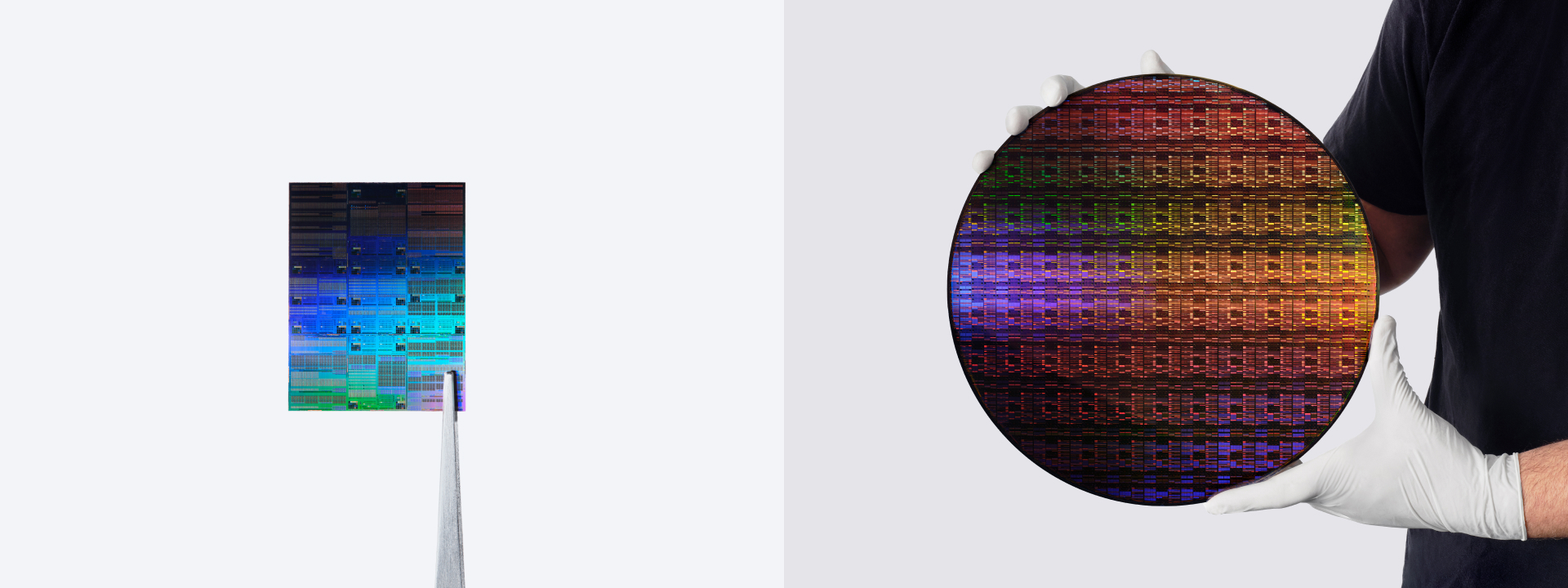
IBM's sub-1 nanometer node chip and wafer.
YORKTOWN HEIGHTS, NY, June 25, 2026 – IBM (NYSE: IBM) today unveiled a major semiconductor breakthrough with the introduction of the world’s first sub-1 nanometer (nm) chip technology, featuring a revolutionary transistor architecture at the 0.7 nm, or 7 angstrom node. The achievement marks a landmark moment for an industry facing the physical limits of traditional chip scaling. Semiconductors play critical roles in everything from computing, to appliances, to communication devices, transportation systems, and critical infrastructure.
IBM’s new sub-1 nm chip packs nearly 100 billion transistors onto a chip the size of a fingernail, nearly twice the density of IBM’s 2 nm chip, unveiled in 2021. Enabled by a series of structural and material innovations, including IBM’s groundbreaking three-dimensional nanostack architecture, the technology demonstrates how continued gains in performance and efficiency remain possible even as chip features approach atomic dimensions.