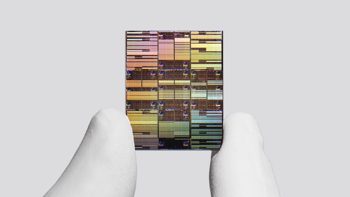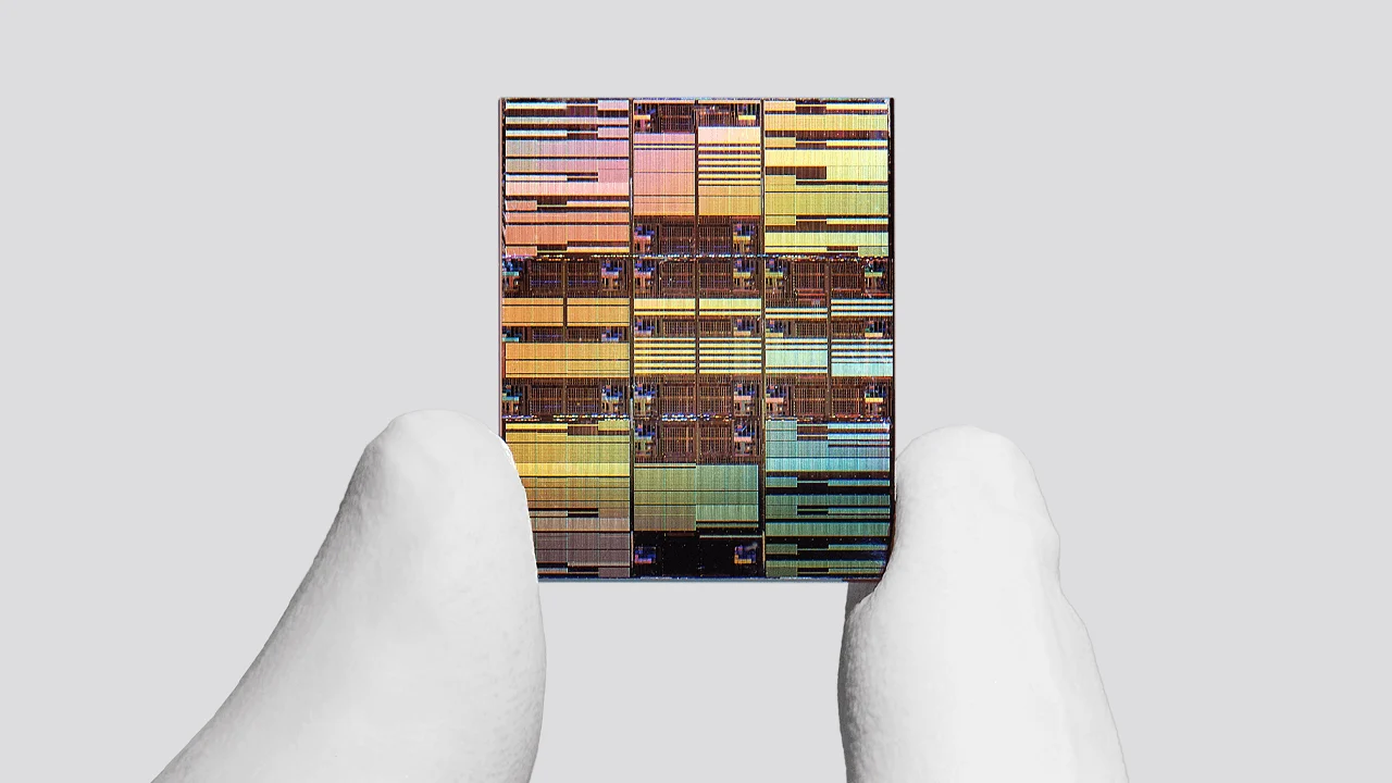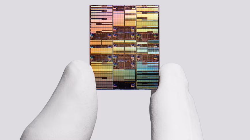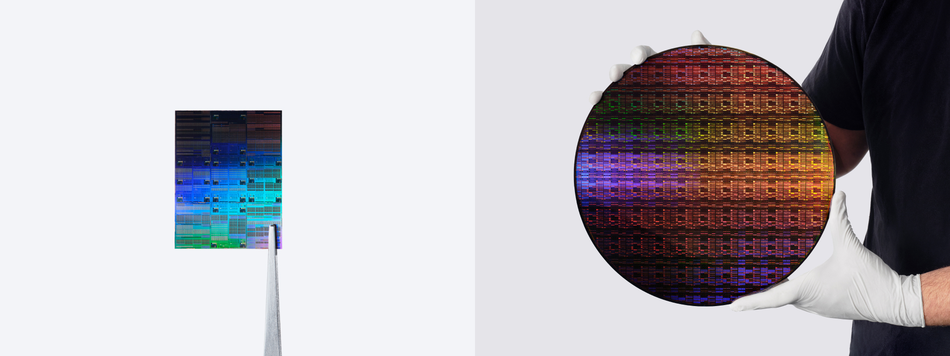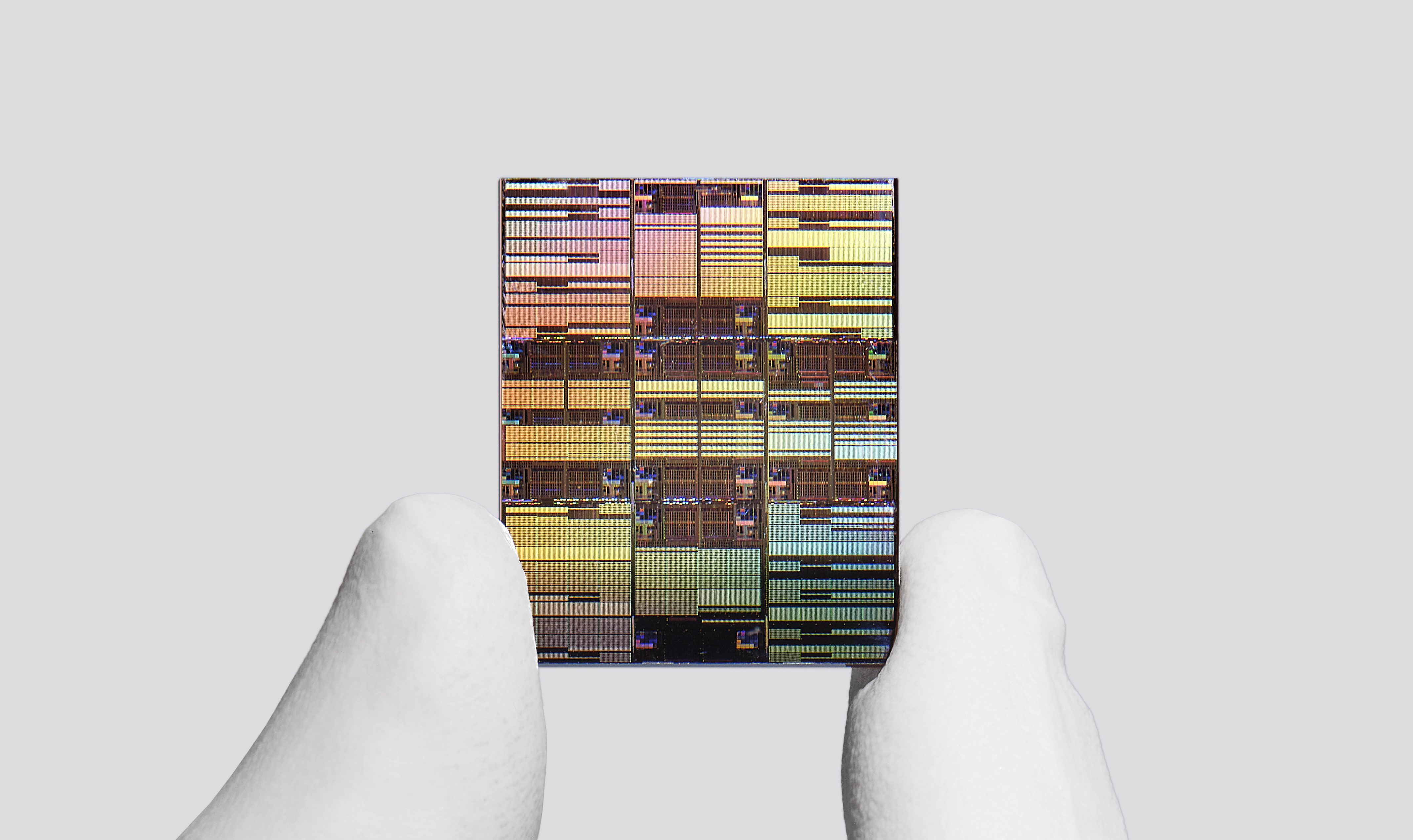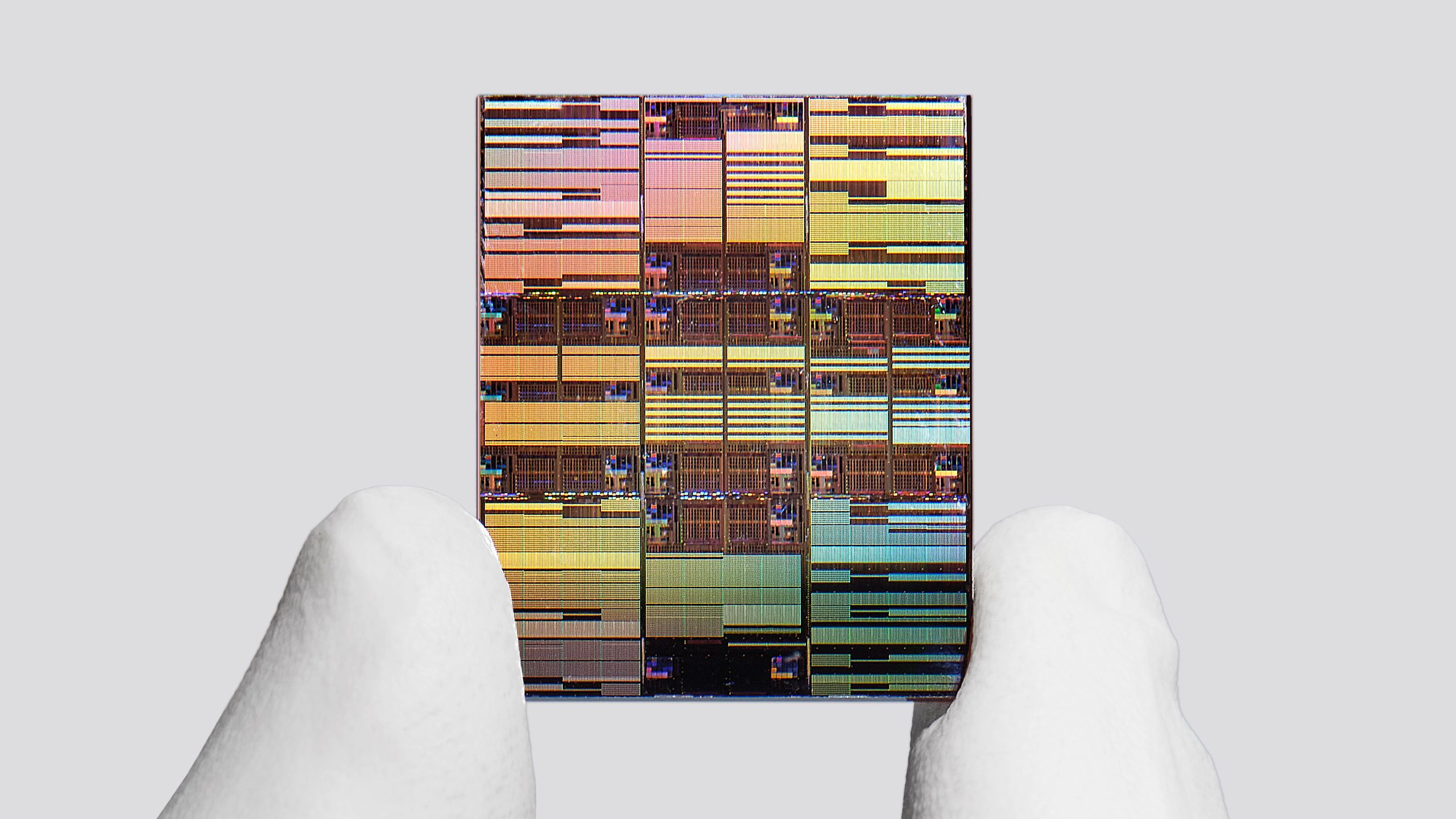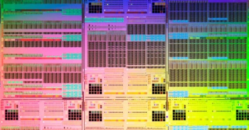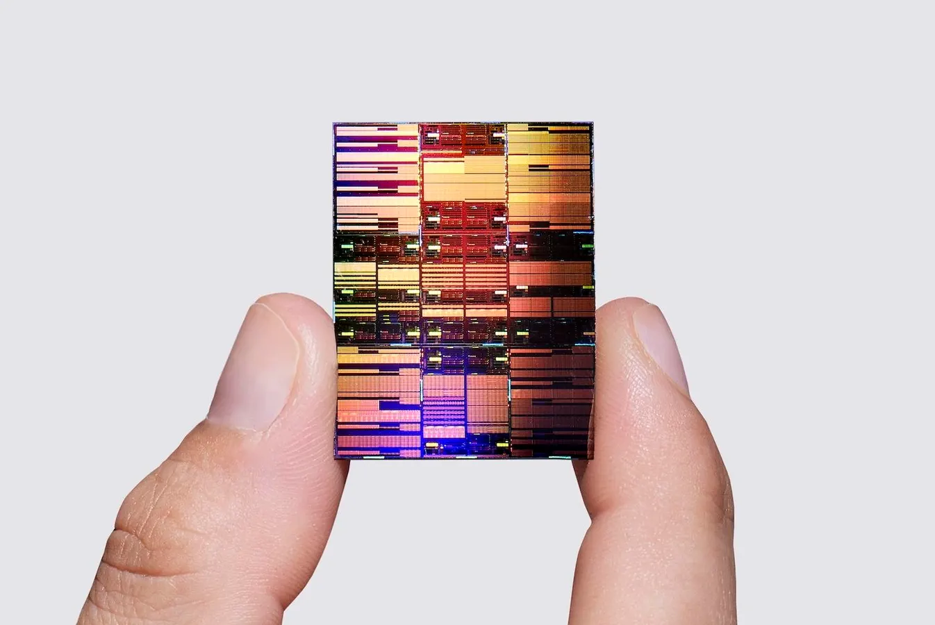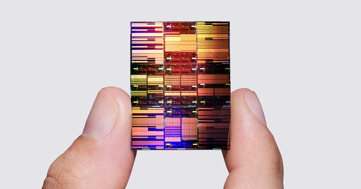
IBM claims to have made a major chip breakthrough with the introduction of the world’s first sub-1nm semiconductor technology.In an announcement detailing the technology, IBM said the ‘nanostack’ 3D architecture features a “evolutionary transistor architecture at the 0.7 nm, or 7 angstrom node,” which will “propel the semiconductor industry forward for the next decade.”The sub-1-nm chips have nearly twice the density of the 2nm chips IBM debuted in 2021, comprising 100 billion transistors and providing up to 50 percent more performance or 70 percent greater energy efficiency for generative AI or cloud applications.IBM says the new nanostack transistor architecture is the industry’s first known three-dimensional, nanosheet-based design, and has been developed by vertically stacking and staggering transistors. The design also uses different material combinations within each stacked layer, optimizing performance and power efficiency of each transistor independent of the other, the company said.IBM went on to add that the architecture was “experimentally validated” through ultra-thin dielectric bonding in CMOS integration, demonstration of dual-channel engineering capability, and functional CMOS inverter operation with expected switching performance.The architecture was developed at IBM’s chip research facility in Albany, New York, which will soon be home to a High Numerical Aperture Extreme Ultraviolet (High NA EUV) lithography tool from ASML.“IBM’s latest chip breakthrough marks a landmark moment in computing, pushing technology beyond the nanometer era to the scale of atoms. With our new nanostack architecture, we’re not just making smaller transistors, we’re reinventing how chips are built to deliver dramatically more power and energy efficiency,” said Jay Gambetta, director of IBM Research and IBM Fellow.“This industry-first innovation continues IBM’s legacy of leading in next-generation technologies and sets the foundation for the next era of computing.”
IBM details major chip breakthrough with new sub-1nm ‘nanostack’ 3D architecture
Company claims technology provides up to 50 percent more performance or 70 percent greater energy efficiency
280 words~1 min read