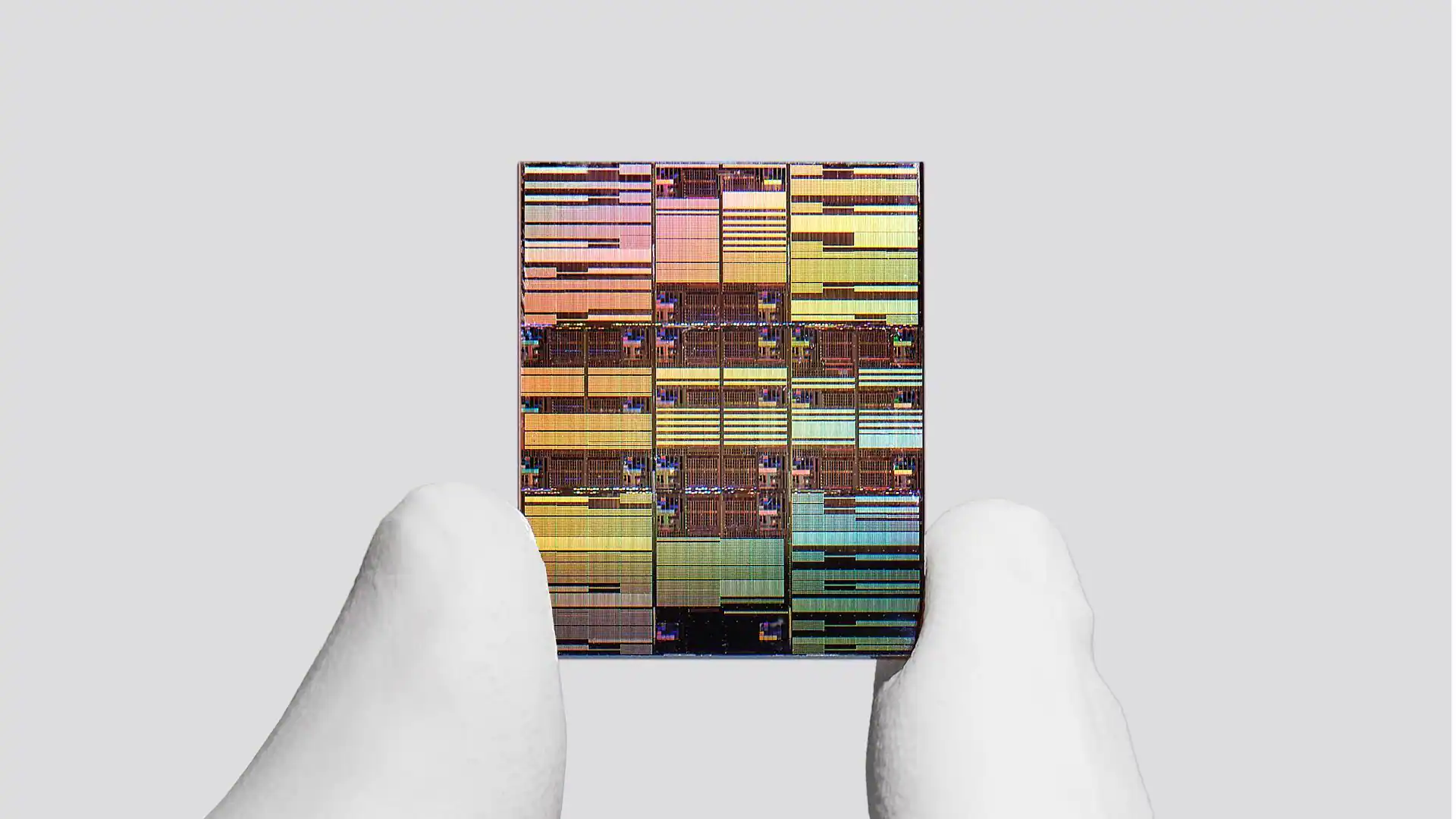
IBM just squeezed roughly 100 billion transistors onto a chip the size of a fingernail. That’s not a typo, and it’s not a theoretical exercise. On June 25, the company unveiled the world’s first 0.7-nanometer chip technology, crossing the sub-1nm threshold that many in the semiconductor world thought was still years away.
To put the scale in perspective: a nanometer is one billionth of a meter. IBM’s new chip operates at 7 angstroms, which is 0.7nm. The technology uses what IBM calls a “nanostack” 3D transistor architecture, a design that stacks components vertically rather than just spreading them across a flat surface.
What the numbers actually mean
IBM’s previous milestone was its 2nm chip technology, introduced back in 2021. The new 0.7nm design nearly doubles the transistor density of that already cutting-edge predecessor.
IBM says the new architecture could deliver up to 50% better performance compared to current 2nm chips. Alternatively, for applications where power consumption matters more than raw speed, the design could achieve 70% greater energy efficiency.