Big Blue shows off process node it claims can scale down to 1 Angstrom
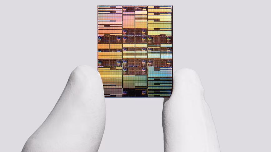
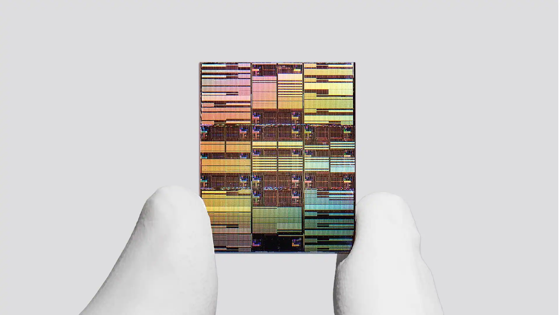
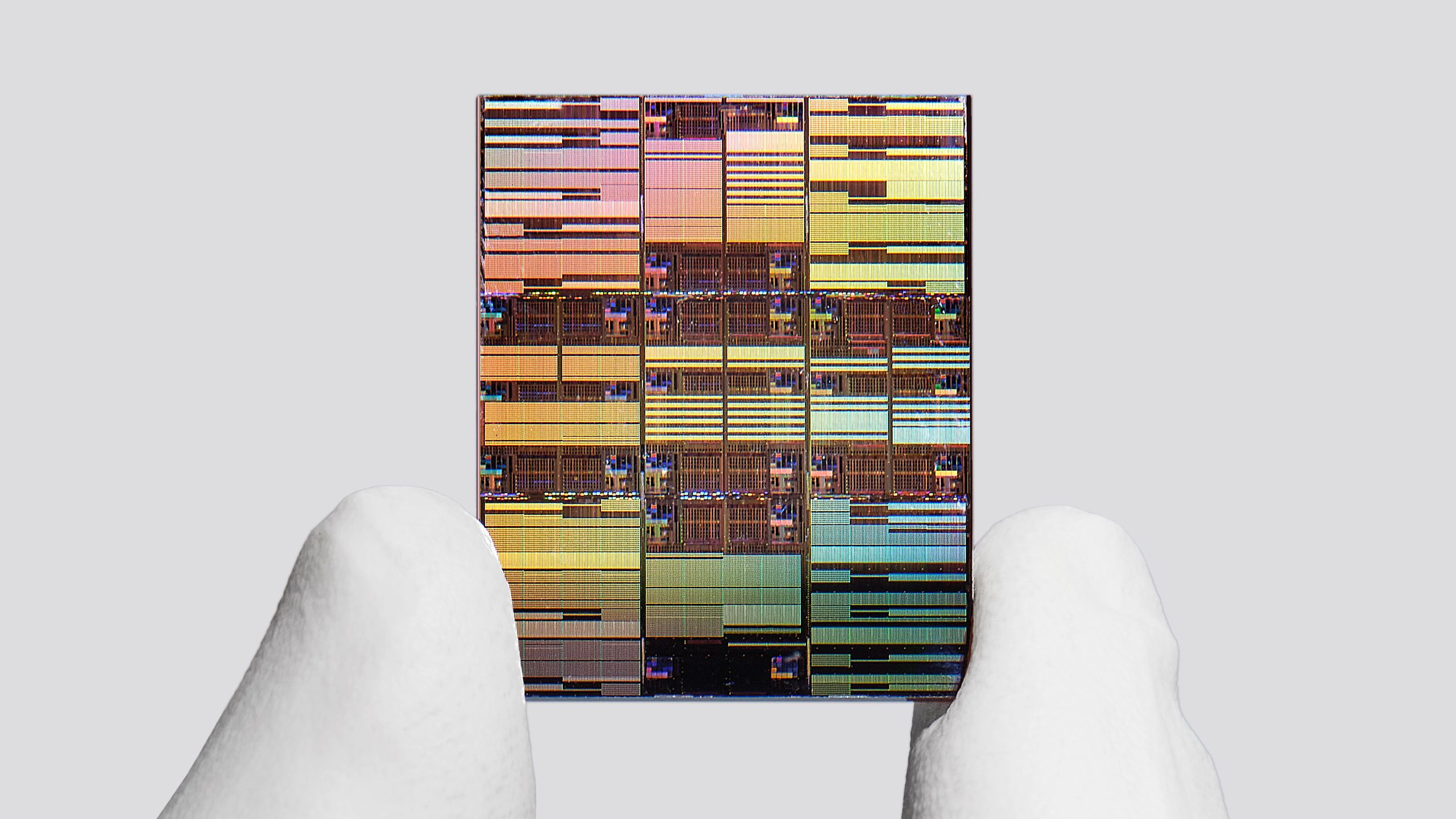
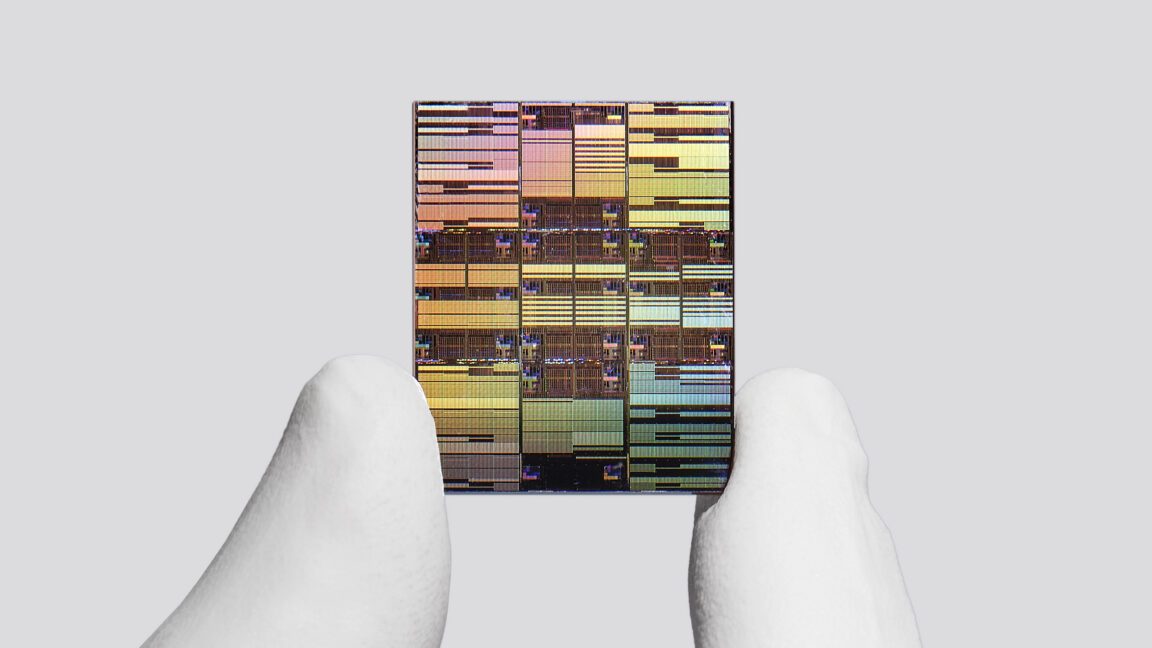
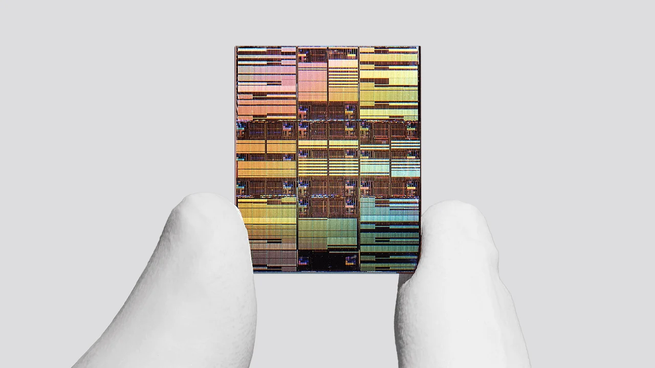
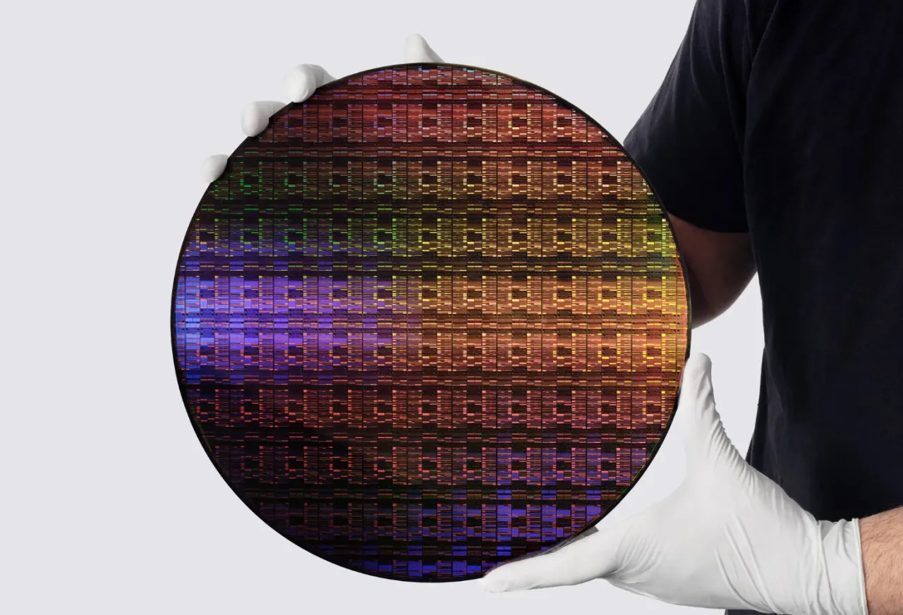
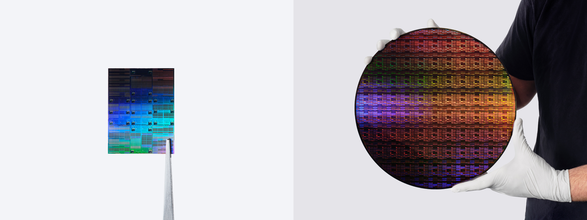
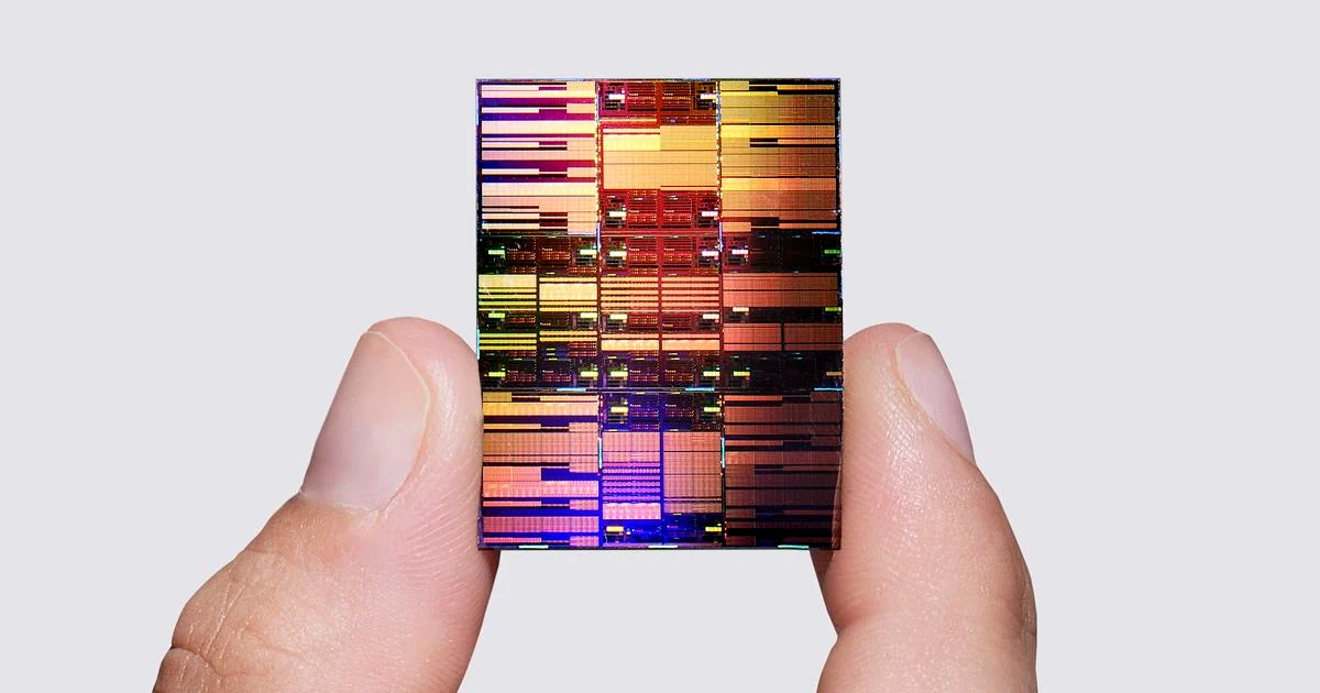
IBM has developed a sub-nanometer (nm) chip technology it says could be used to produce commercial chips within five years, and has mapped a path to 0.1 nm.Big Blue claims its new process node can cram nearly 100 billion transistors onto a silicon die the size of a fingernail, almost double the density of the 2 nm technology it unveiled back in 2021.The new process as disclosed is actually for 0.7 nm or 7 Angstroms (7A), compared with the cutting-edge manufacturing nodes now being prepared for production in 2028 by the likes of Intel and TSMC which are 1.4nm, or 14 Angstroms.
Several structural and material innovations have gone into this latest manufacturing method, including a three-dimensional nanostack architecture that sees transistors stacked, with n-type and p-type field-effect transistors (FETs) arranged so that one is layered above the other.
"We're announcing it's not just an incremental step, it's a meaningful leap forward, enabling up to 50 percent higher performance, or 70 percent greater efficiency [than 2nm], and pointing to a future where computing becomes significantly more powerful without a corresponding increase in energy," claimed director of IBM Research and IBM Fellow Jay Gambetta.And the firm sees a clear path to shrinking down to one-tenth of a nanometer over the next ten years, he added."Nanostack is not one innovation. It is actually a device platform that can enable the future of scaling for another decade beyond nanosheet, as you can see from our technology roadmap all the way to 1 Angstrom."