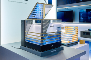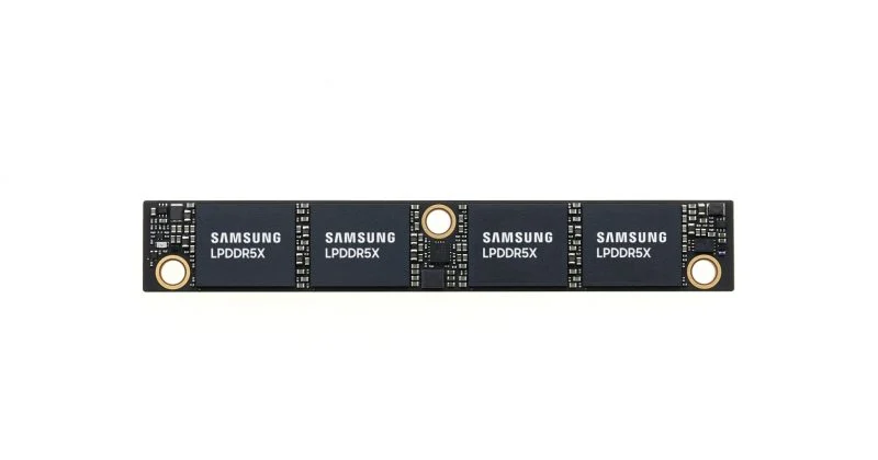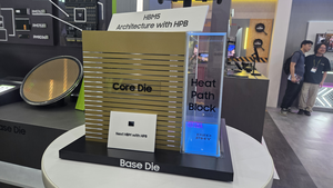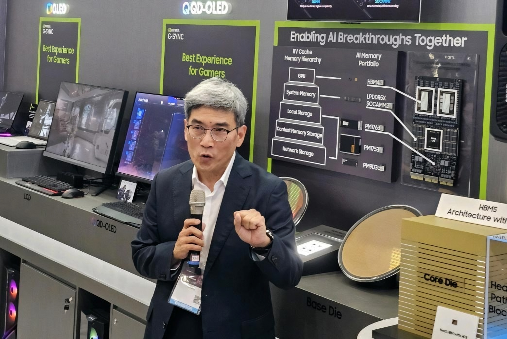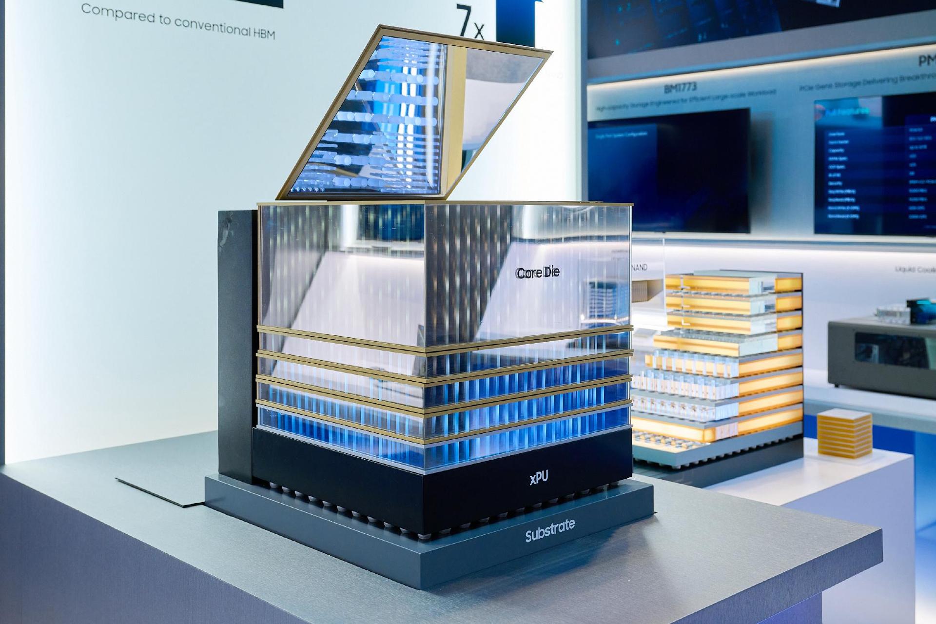
A mockup of Samsung Electronics' zHBM is displayed at its booth for the Future of Memory and Storage 2026 in California, Tuesday (local time). Courtesy of Samsung Electronics
Samsung Electronics showcased its next-generation 3D memory architectures at the Future of Memory and Storage 2026 in California on Tuesday (local time), unveiling mockups of zHBM and zNAND-O.
Samsung outlined its vision for 3D architectures for future memory solutions during a keynote speech by its memory business executives and exhibited mockups of the two new structures at its booth.
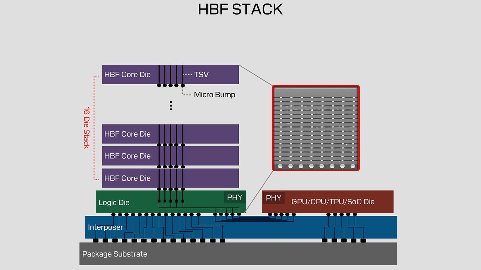
ZHBM is an architecture aimed at improving the data processing speed of artificial intelligence (AI) accelerators by shortening the physical distance between logic processors — central processing units, graphics processing units and others — and high-bandwidth memory (HBM).
While conventional HBM is placed beside logic chips, zHBM is stacked directly on top of the processor. By shortening the distance that data must travel, the new architecture delivers higher bandwidth and improved power efficiency.