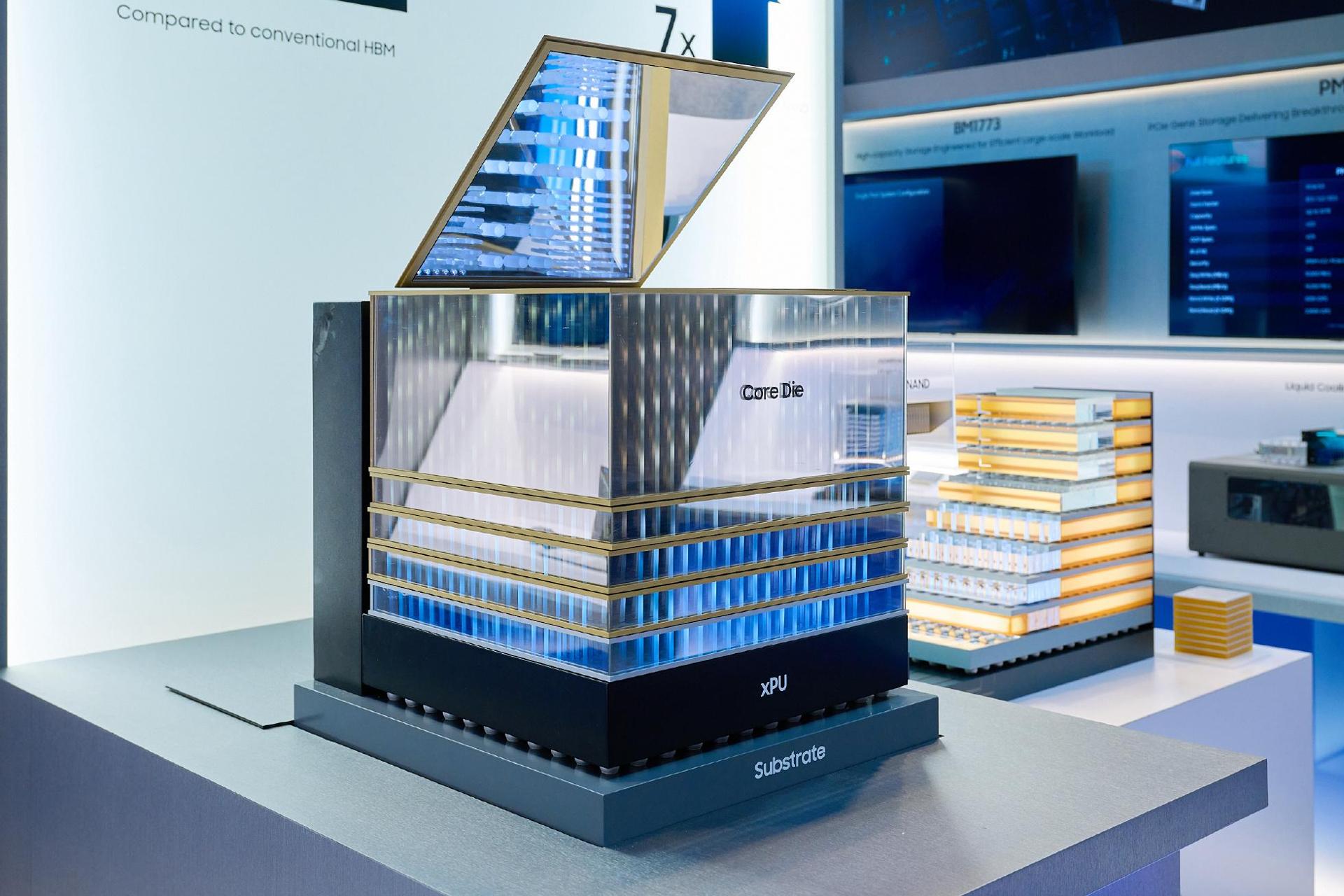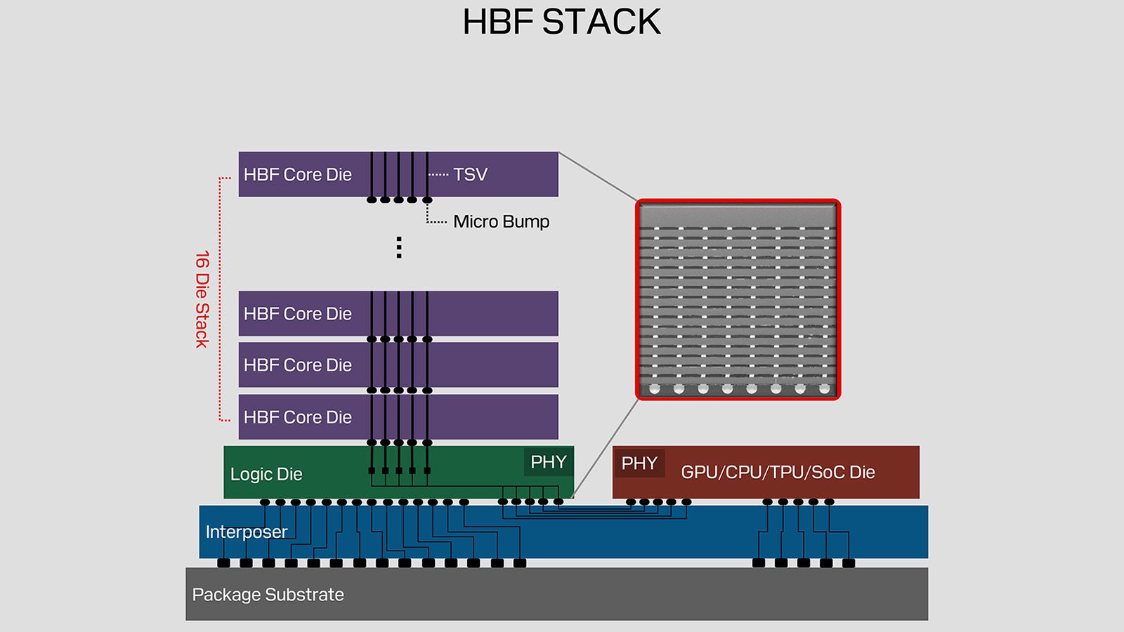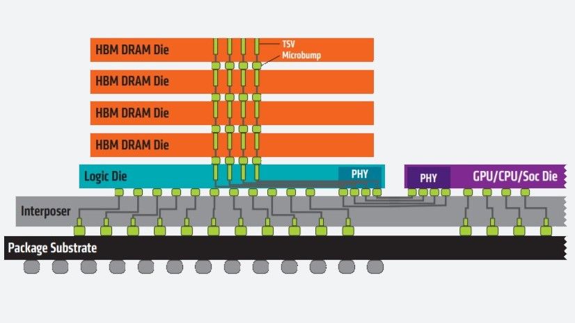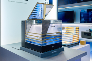
Industry-first zHBM promises up to eightfold performance, new NAND designs target on-device AI A concept model of Samsung Electronics’ zHBM on display at the company’s booth during the Future of Memory and Storage 2026 in California on Tuesday. (Samsung Electronics) Samsung Electronics is placing high-bandwidth memory directly on top of AI processors, unveiling a 3D architecture that requires less power to deliver faster data transfers.The tech giant is showcasing concept models of the architecture, called zHBM, and a NAND flash solution dubbed zNAND-O at Future of Memory and Storage 2026, held from Tuesday to Thursday at the Santa Clara Convention Center in California.Samsung described the two concept models as industry firsts.Conventional HBM packages are placed alongside graphics processing units and other AI accelerators on the same plane. The zHBM design instead positions the memory above the processor, reducing the physical distance over which data must move.The design is intended to ease data bottlenecks in AI systems, where processors must continuously exchange large volumes of information with memory. The shorter connection could increase bandwidth while reducing the power used.Samsung said a next-generation interface system incorporating zHBM could deliver up to eight times the performance of HBM5, the eighth-generation HBM. Energy efficiency could improve by as much as threefold.The company said advanced wafer bonding technology could also cut thermal resistance by more than half compared with HBM5, addressing one of the main challenges of vertically stacking high-performance memory and processors.The architecture can be tailored to individual AI systems through an interlayer between the memory and accelerator that incorporates customer-specific intellectual property. Depending on the system design, the interlayer could be configured to expand memory capacity or enhance processor performance.Samsung said it would work with customers to optimize the connection between their AI processors and memory and further improve zHBM performance. It did not disclose a timetable for commercialization.The company is also extending its 3D memory approach to NAND flash.The zNAND-O solution, which remains under development, combines Samsung’s V-NAND stacking technology with through-silicon vias, or TSVs. Four or eight semiconductor dies are stacked vertically and packaged as a single product.The “O” in the name denotes its focus on on-device AI, where data is processed locally rather than sent to an external server.By stacking the dies, Samsung aims to reduce the amount of space occupied by the memory while improving data-loading bandwidth and response times. The solution is designed for devices that must process large volumes of data locally and in real time.At the event, Samsung also unveiled V10 BV-NAND, its 10th-generation V-NAND technology featuring more than 400 vertically stacked memory-cell layers.The company described it as the industry’s first V-NAND design to surpass the 400-layer mark.The higher-density structure allows more memory cells to be placed within the same area, increasing storage capacity while improving performance and power efficiency.The announcement comes 13 years after Samsung introduced what it described as the world’s first V-NAND technology at the same industry event.Samsung plans to use the new 3D memory technologies to address growing demand for high-performance computing and AI infrastructure.
Samsung stacks HBM atop AI chips in 3D memory push
Samsung Electronics is placing high-bandwidth memory directly on top of AI processors, unveiling a 3D architecture that requires less power to deliver faster da
504 words~2 min read