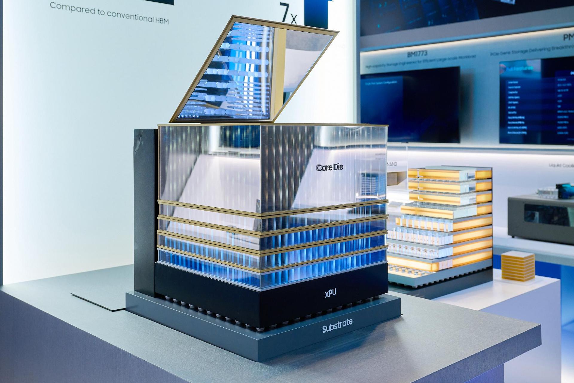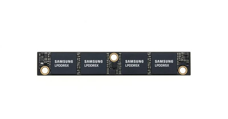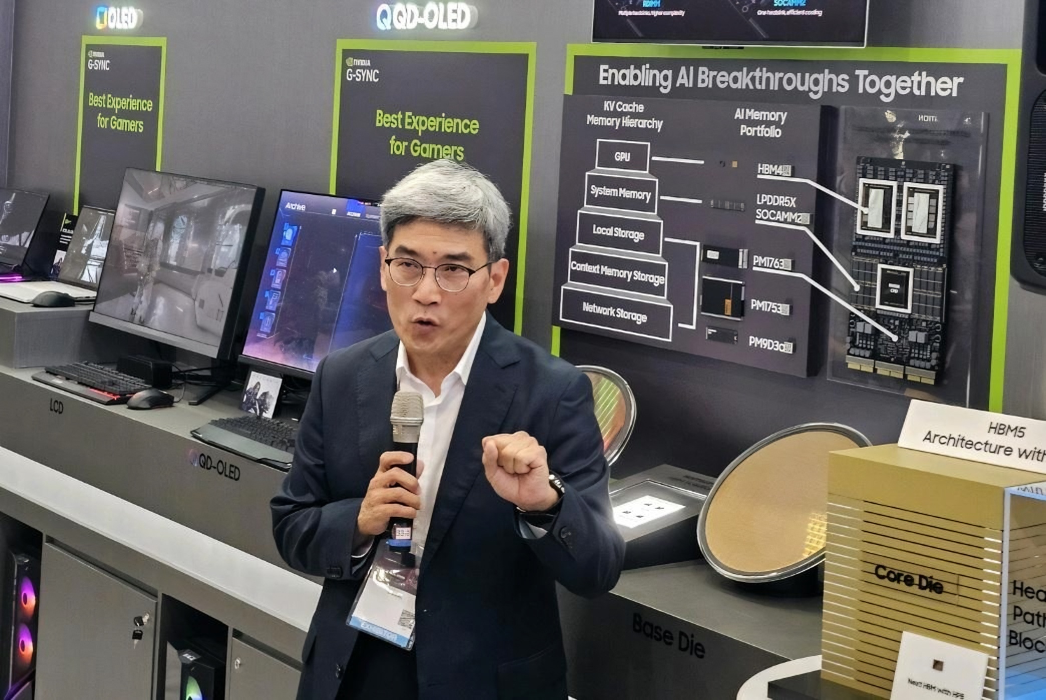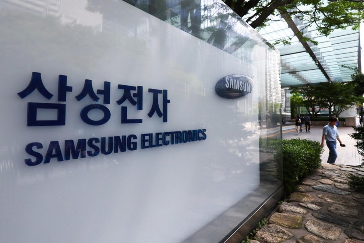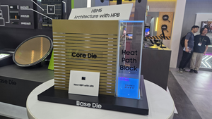
Samsung Electronics Co. said Wednesday that it unveiled the industry's first concept models of zHBM, a next-generation memory architecture expected to deliver approximately eight times the performance of HBM5. The logo of Samsung Electronics is seen at the technology company's store in Seoul, South Korea, April 15, 2025. (Reuters-Yonhap) The world's largest memory chipmaker showcased the next-generation technology at the Future of Memory and Storage 2026 conference in Santa Clara, California, on Tuesday (local time).Designed for advanced artificial intelligence (AI) computing, zHBM features a new memory architecture that vertically stacks high-bandwidth memory (HBM) directly above AI accelerators, moving beyond conventional designs in which HBM is positioned alongside the processor.Using wafer-bonding technology, zHBM can also achieve more than 10 times the memory density of HBM5 while tripling energy efficiency and reducing thermal resistance by more than half, according to the company.The technology also supports customer-specific designs by allowing customized intellectual property to be integrated into the interlayer between the memory and AI accelerator, expanding memory capacity and improving accelerator performance.By minimizing the distance data travels between the AI processor and memory, zHBM is designed to provide higher bandwidth and greater power efficiency, enabling the ultra-fast data processing required for large-scale AI training and inference.Building on its close collaboration with customers, Samsung Electronics said it plans to further optimize the integration of AI processors and memory through zHBM to maximize AI system performance. (Yonhap)
Samsung unveils industry's 1st zHBM concept, targeting 8-fold HBM5 performance
Samsung Electronics Co. said Wednesday that it unveiled the industry's first concept models of zHBM, a next-generation memory architecture expected to deliver a
232 words~1 min read