HomeAI · summaries
Storia in 18 fonti
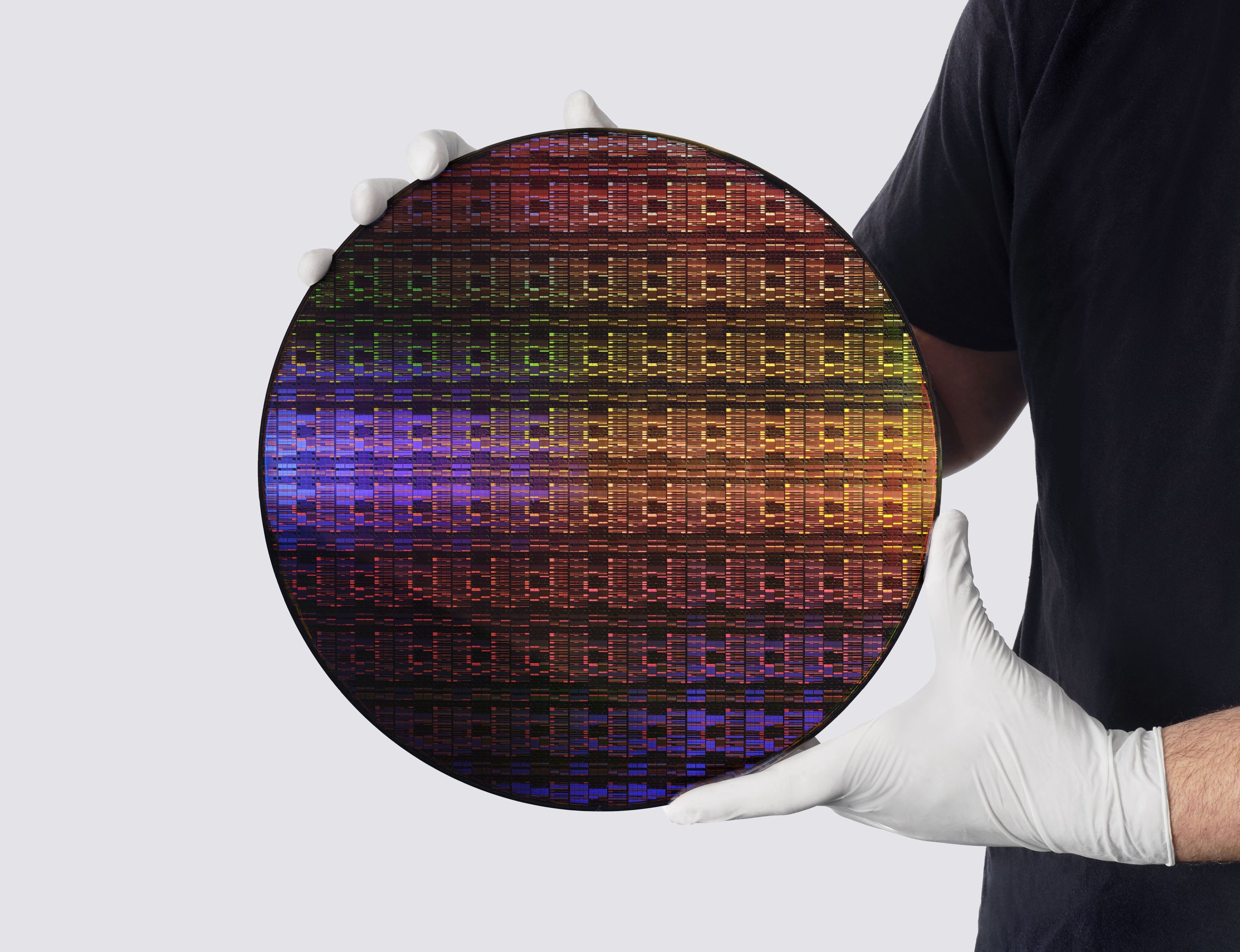
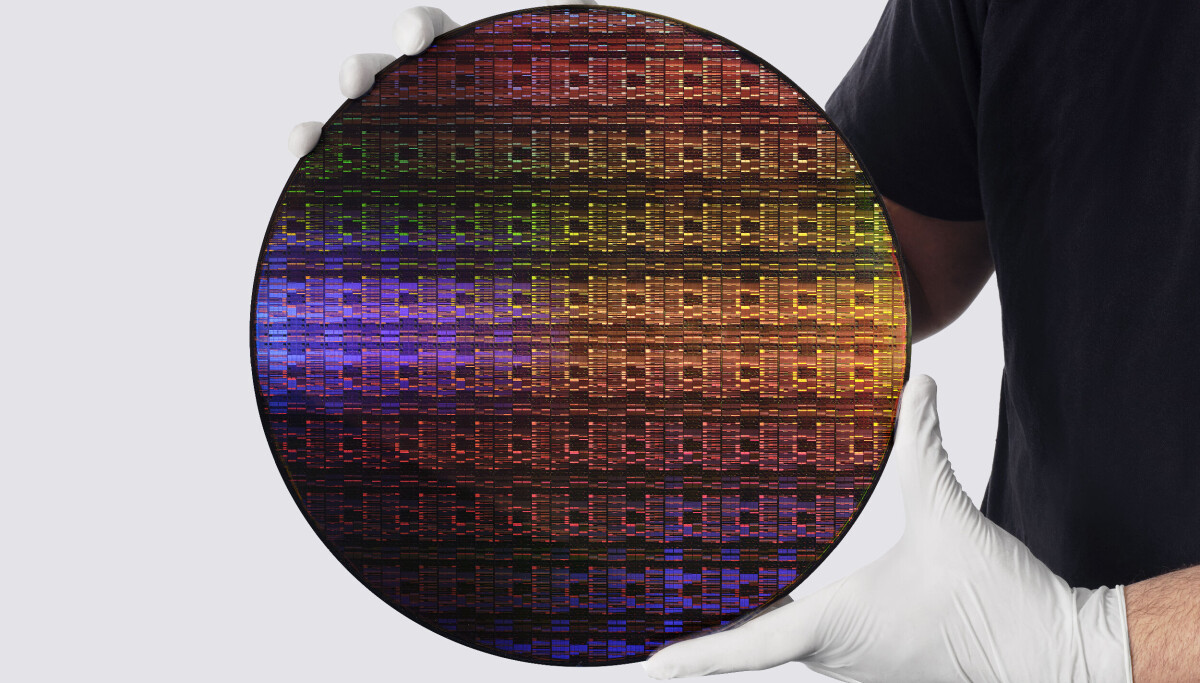
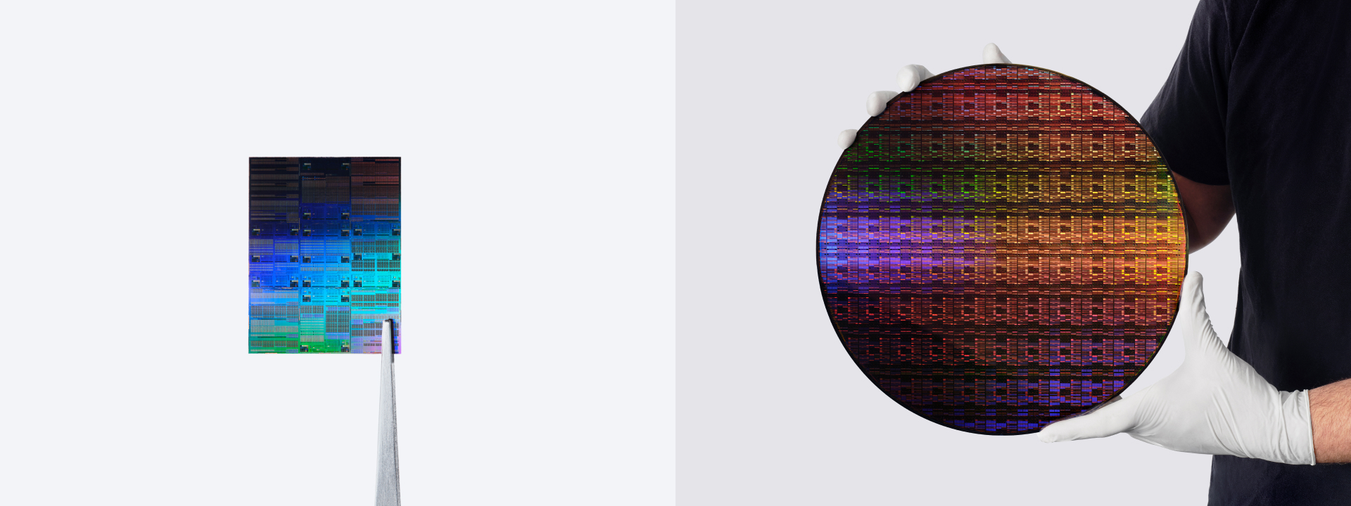
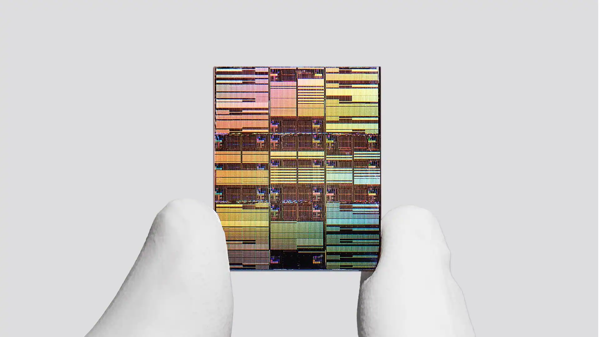
IBM rompe la barrera del nanómetro con un chip de nueva generación
La tecnología nanostack mejora el rendimiento y la eficiencia energética para responder a la creciente demanda de IA
Confronto fonti
6 prospettive sulla stessa storiaTimeline cronologica
- ·
datacenterdynamics.com
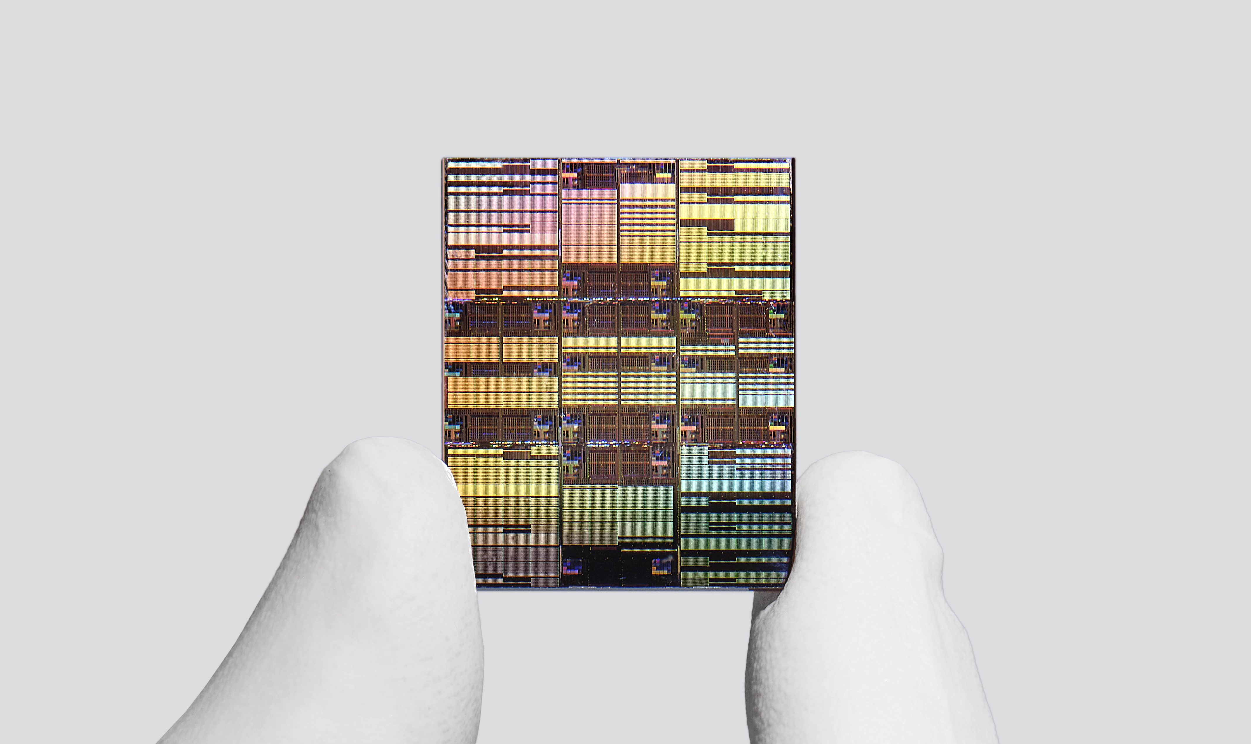
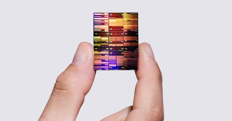
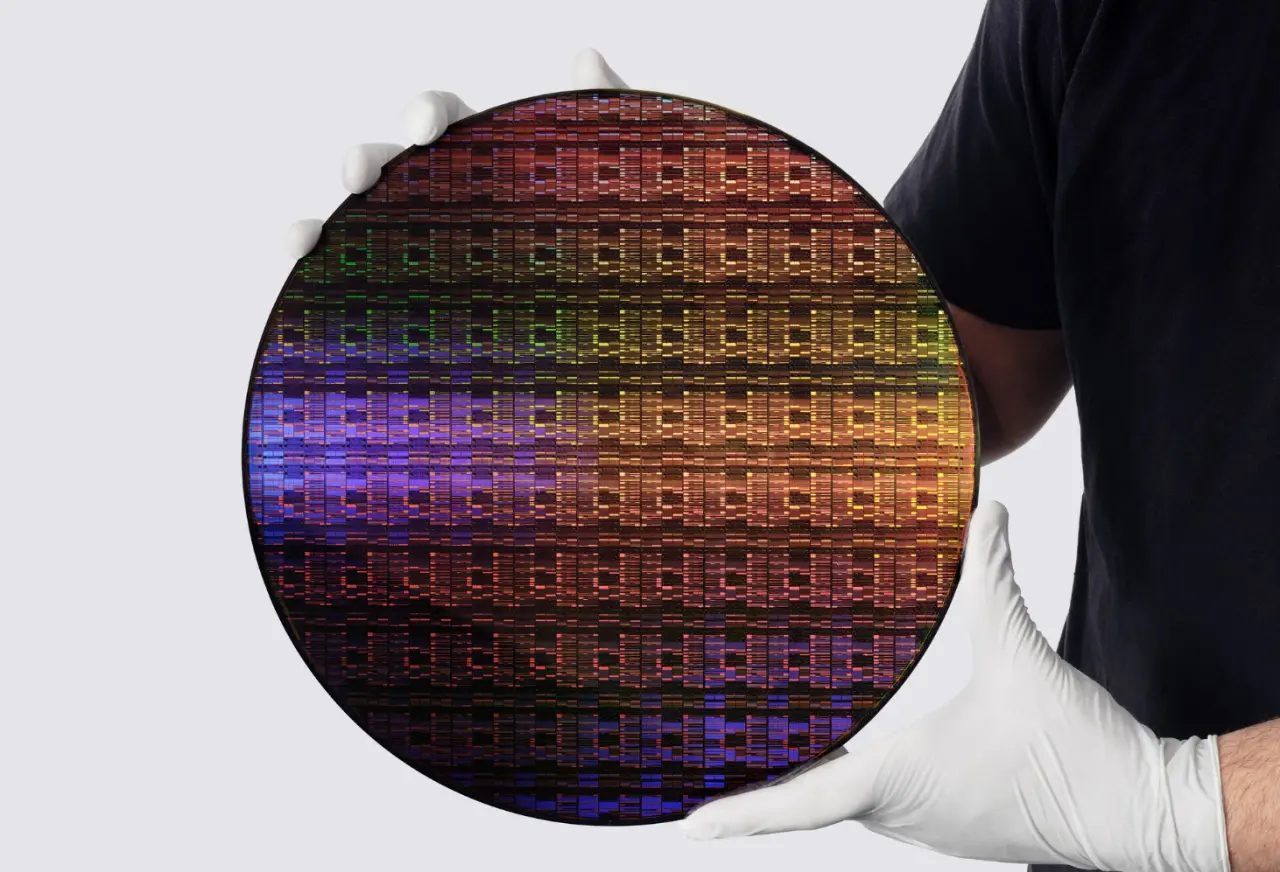
IBM details major chip breakthrough with new sub-1nm ‘nanostack’ 3D architecture
Company claims technology provides up to 50 percent more performance or 70 percent greater energy efficiency
- ·
forbes.com
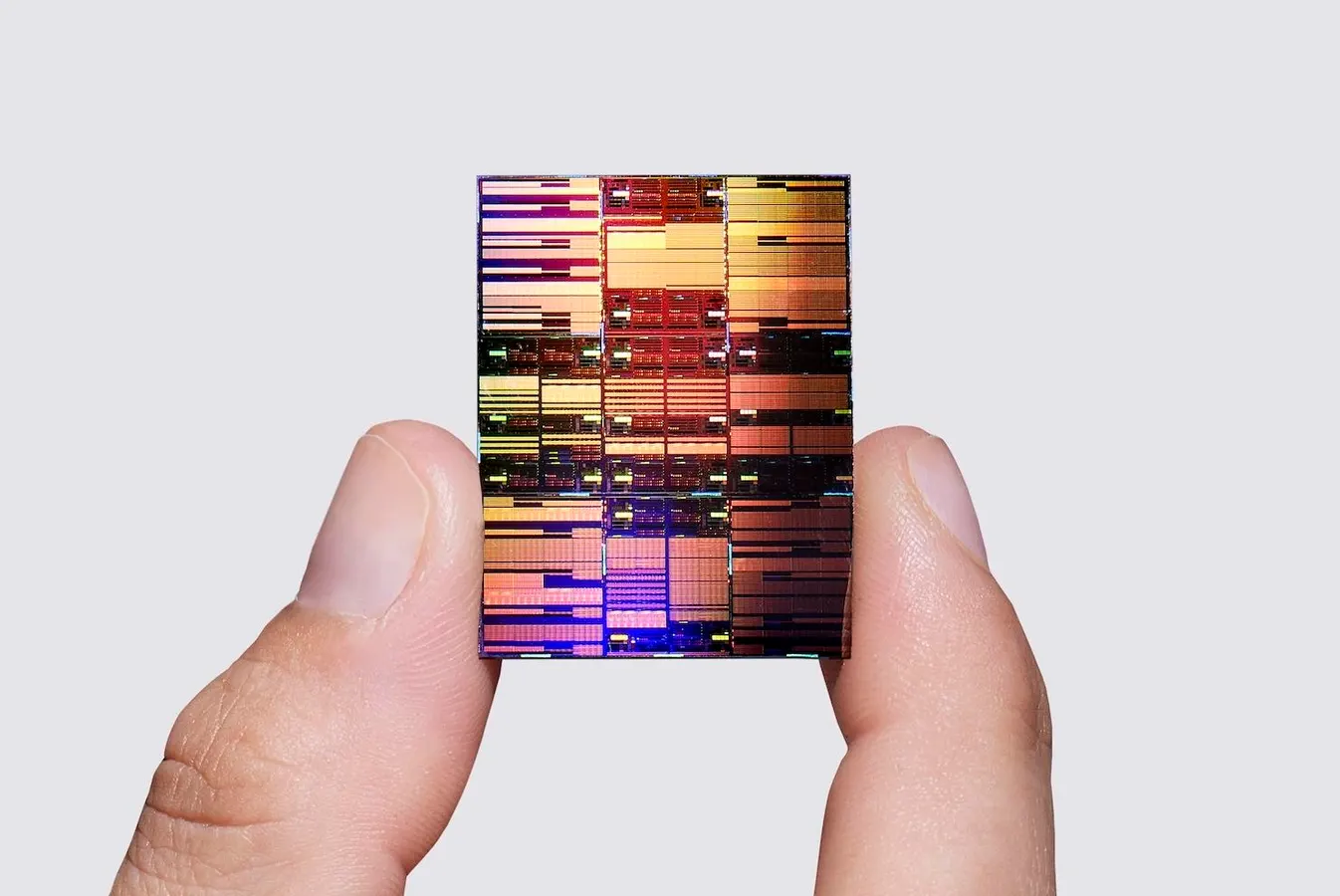
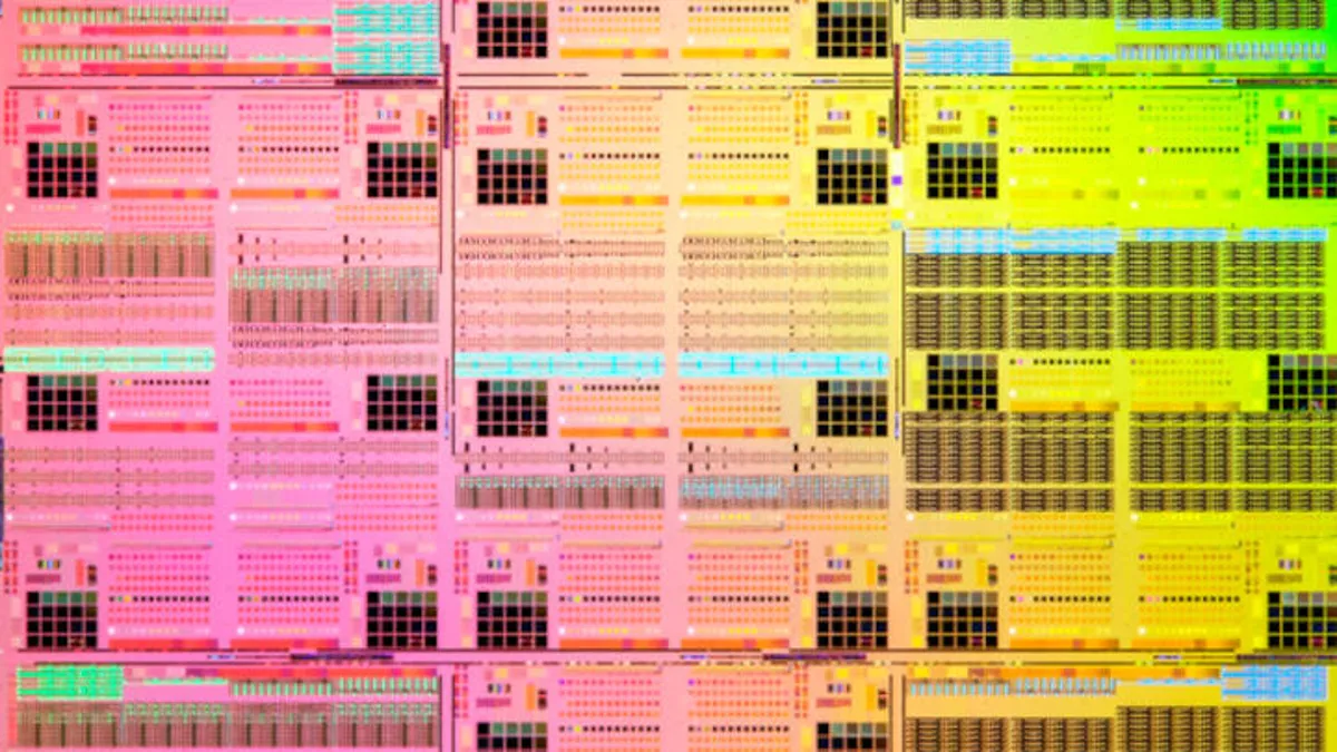
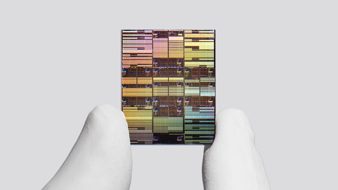
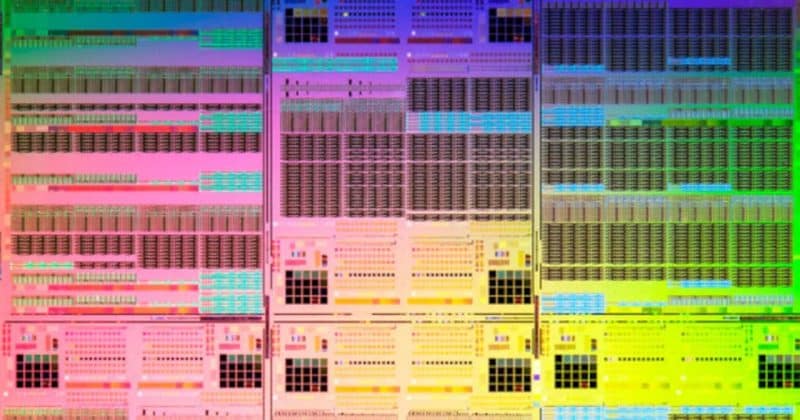
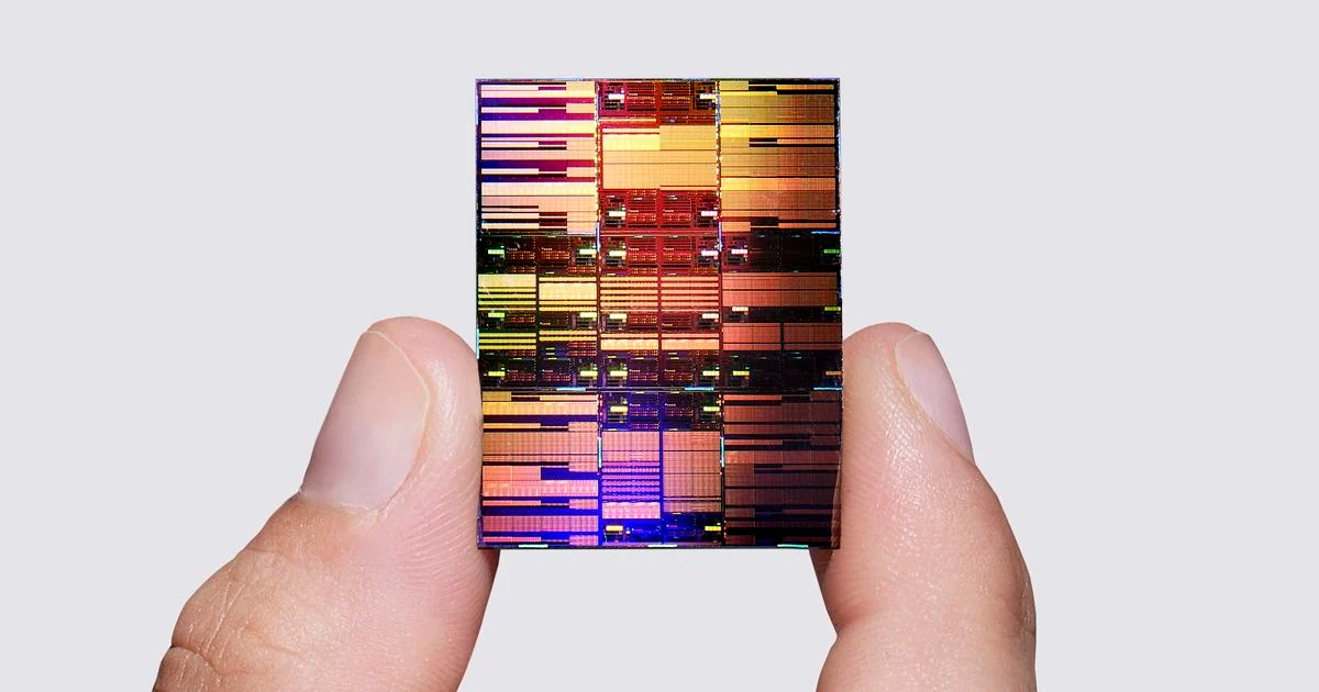
IBM Unveils World’s First Sub-1nm Chip With 100 Billion 3D-Stacked Transistors
IBM just unveiled the world's first sub 1-nanometer chip: 100 billion transistors. IBM also says they've produced functioning devices with this technology.