(Image credit: Samsung)
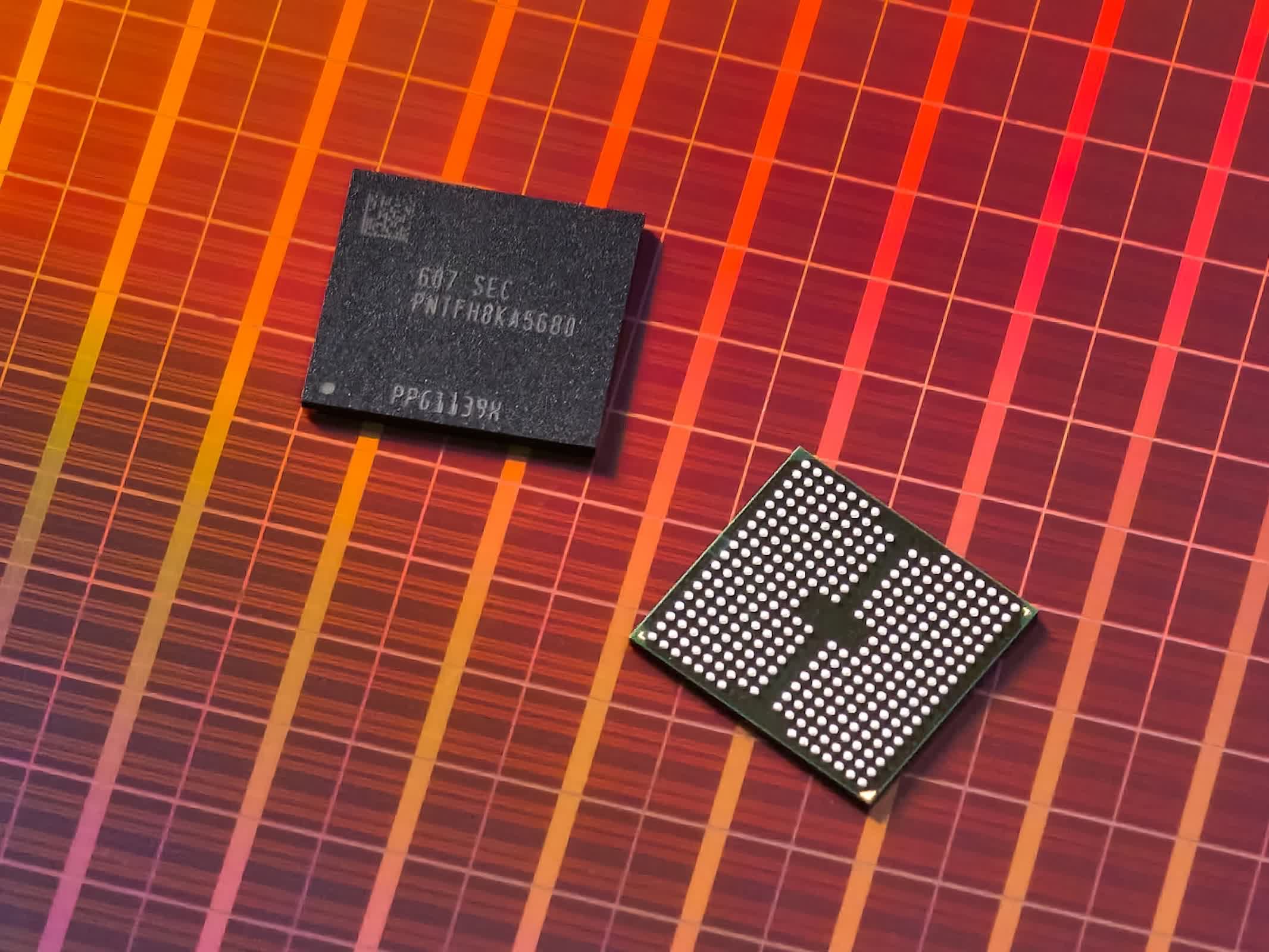
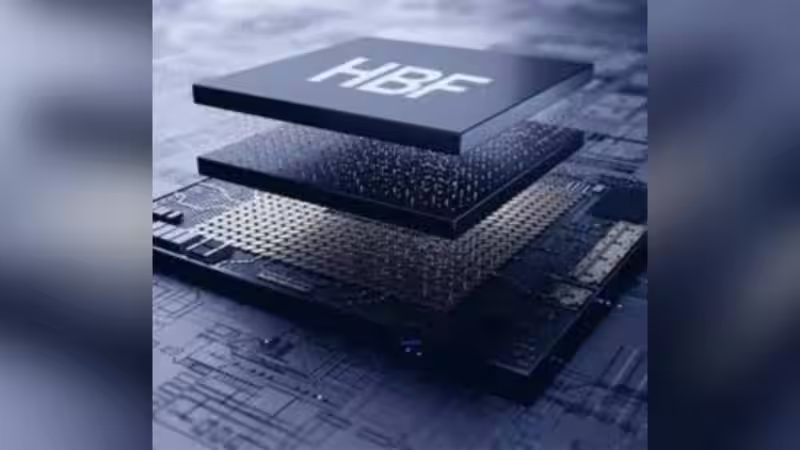
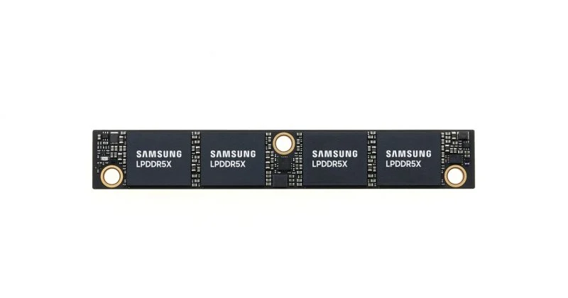
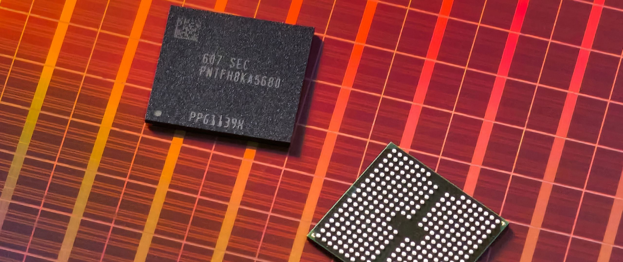
This week, Samsung presented its vision for next-generation memory and storage solutions both for AI and general-purpose applications at the Future of Memory and Storage (FMS) 2026 conference. The company introduced zHBM, zNAND-O, and BV-NAND technologies at the event, and while they are aimed at very different applications, they share one common ingredient: they all rely on wafer bonding.Here's a breakdown of each type of technology that the company announced.zHBM: Samsung’s vision for custom HBM ultra-high-performance memory that will sit on top of logic dies.zNAND-O: NAND memory that can be bonded atop a logic device to maximize bandwidth, reduce latency, and minimize power consumption.BV-NAND (aka Samsung’s 10th Generation V-NAND): Samsung’s take on bonding NAND arrays atop all the circuitry needed to operate them. This is essentially next-generation 3D NAND technology that is used today by almost everyone, including Kioxia/Sandisk, SK Hynix, and YMTC (which was the first company to adopt such a method).
Disclaimer
This article is a preview of the type of content that readers can expect from our subscription service, Tom's Hardware Premium. If you're interested in more technical content that spans across the hardware industry, subscribe for as little as $29 per year, or $7 per month.