Serving tech enthusiasts for over 25 years.
TechSpot means tech analysis and advice you can trust.
In brief: Samsung is adding a new set of memory technologies to its AI strategy, using wafer bonding and 3D stacking to push bandwidth, density, and energy efficiency beyond what current high-bandwidth memory and NAND technologies can deliver.
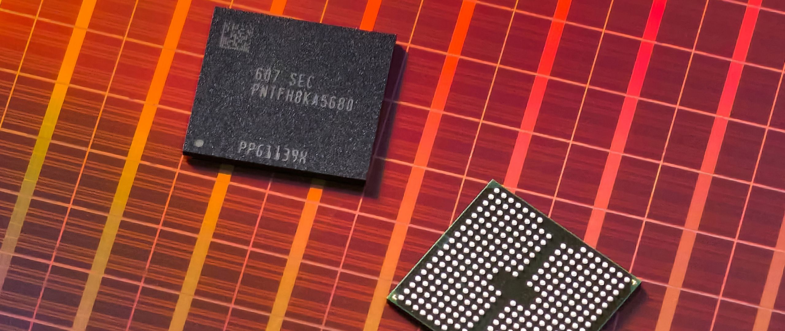
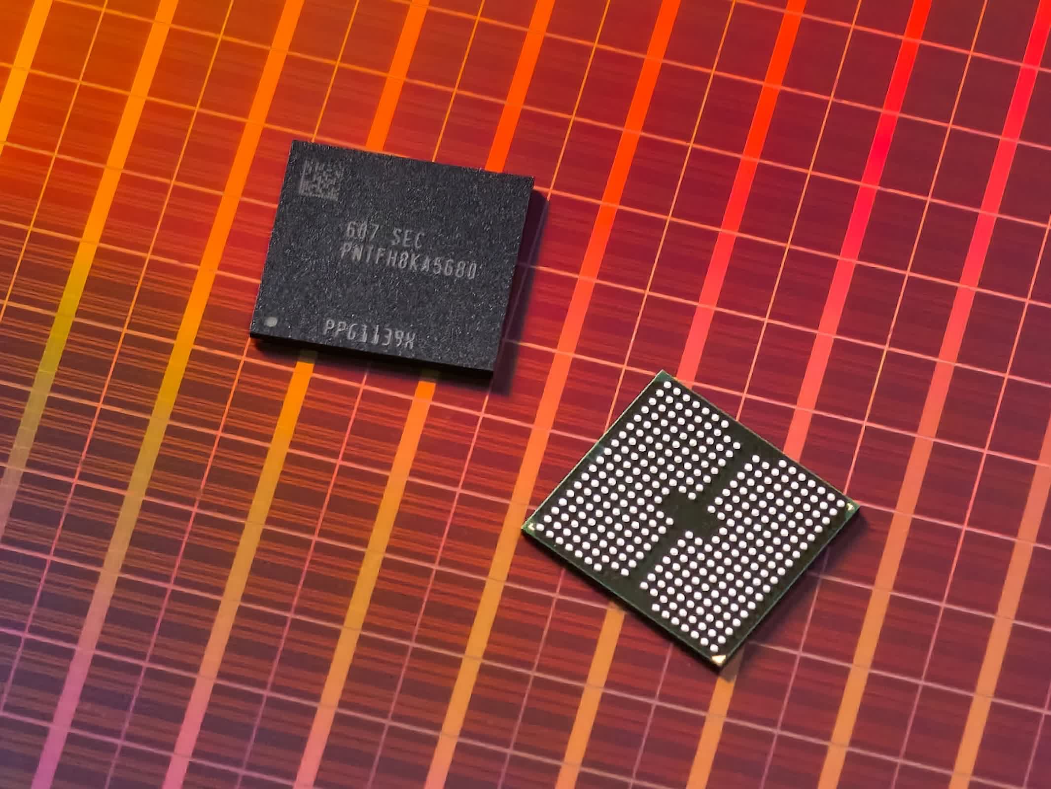
At the Future of Memory and Storage 2026 conference in Santa Clara, California, the company laid out a roadmap built around three main technologies: a new Bonding V-NAND architecture with more than 400 layers, a concept for vertically stacked high-bandwidth memory called zHBM, and a next-generation NAND approach called zNAND-O. These technologies target both large-scale AI training workloads in data centers and edge AI applications that require low latency and tight power controls.
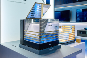
A key part of that strategy is zHBM, a new way of arranging high-bandwidth memory. In today's systems, HBM usually sits next to AI processors. zHBM instead stacks HBM directly on top of AI accelerators, placing the memory above the compute. This design shortens the physical distance data has to travel between the processor and memory, which is intended to increase bandwidth and improve power efficiency for large-scale AI training and inference.