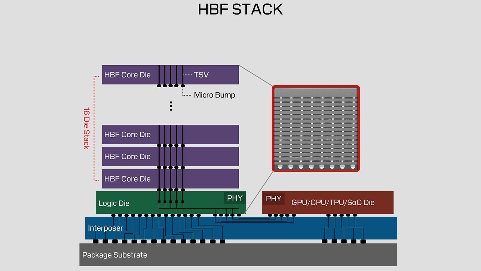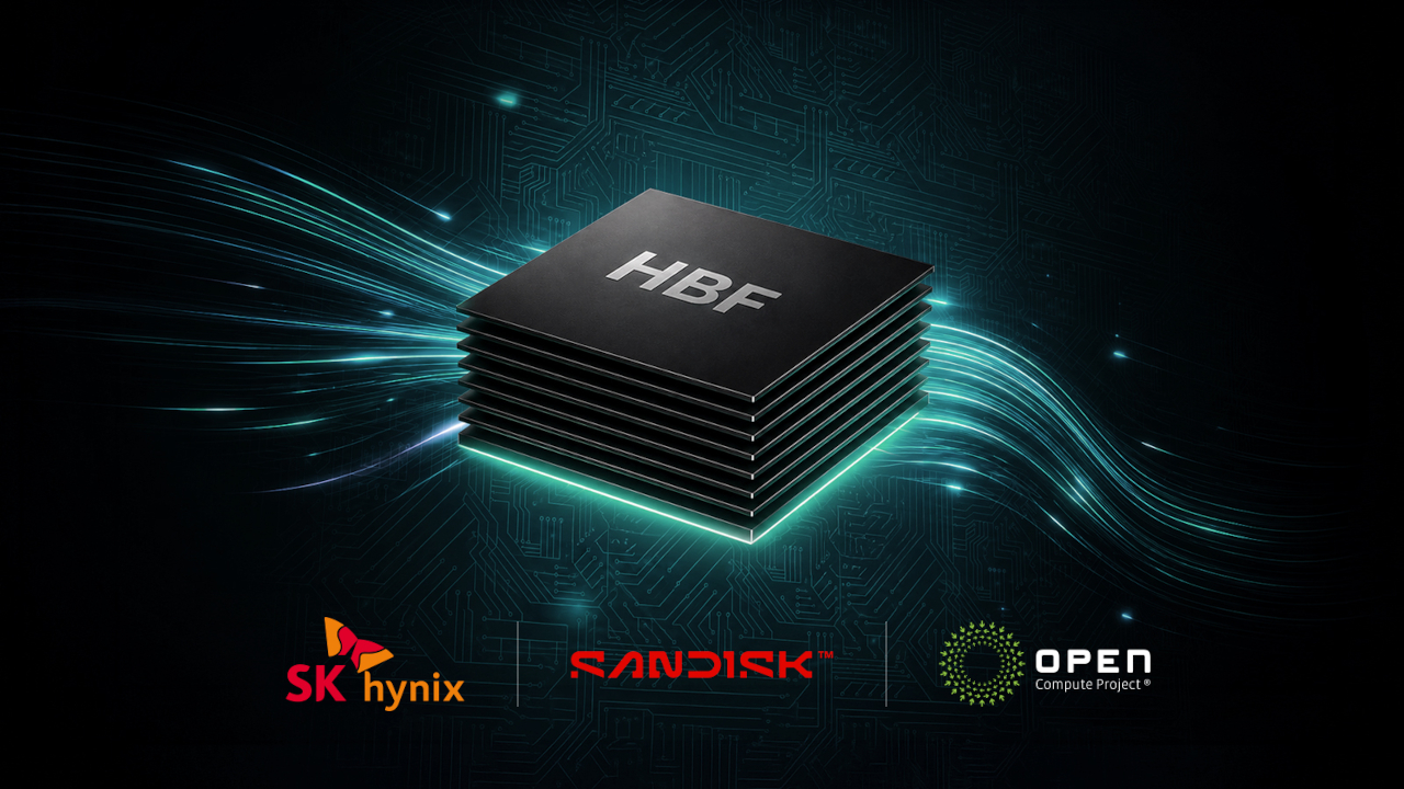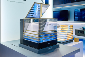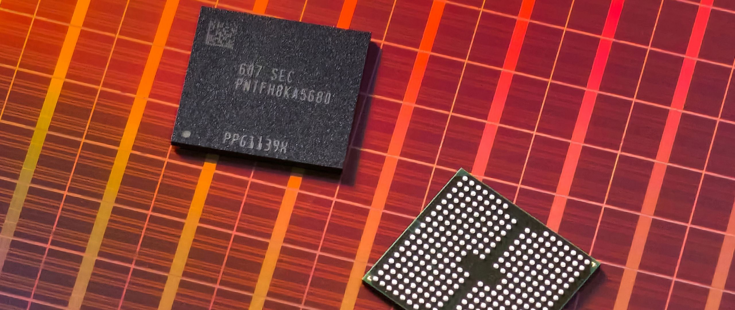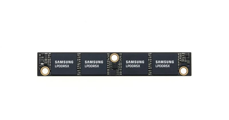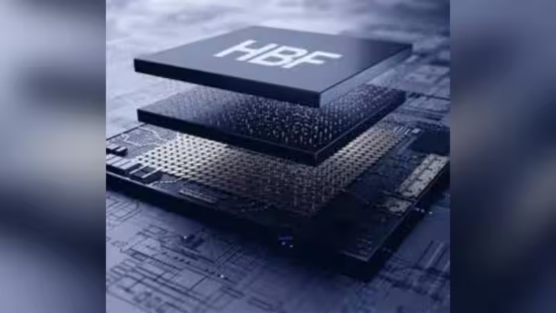
The race to build faster and higher-capacity memory for AI systems is moving beyond traditional High Bandwidth Memory (HBM). Sandisk and SK hynix have now formally introduced the High Bandwidth Flash (HBF) specification, a new storage technology designed to combine the capacity and non-volatility of 3D NAND with performance closer to that of HBM.The companies are positioning HBF as a new memory tier for AI inference workloads, where the amount of data that needs to stay close to the compute hardware is growing rapidly. At the same time, Samsung is exploring a different route to tackle the same challenge, with new 3D memory and NAND technologies showcased at Future of Memory and Storage (FMS) 2026.About The AuthorJournalist and a writer with a strong interest in news, culture, technology, and human-interest stories. Passionate about making complex topics accessible and engaging.Together, the developments highlight how memory architecture is becoming increasingly important as AI systems demand more bandwidth, capacity and power efficiency.Sandisk and SK hynix's HBF can offer up to 512GBThe initial HBF specification, released through the Open Compute Project (OCP), defines packages with capacities of up to 512GB. These will use either 8-Hi or 16-Hi NAND die stacks, although they will not be standard 3D NAND stacks. Instead, the companies are working with specialised devices featuring a faster interface. Sandisk has previously referred to these as HBF core dies.HBF will be offered across three bandwidth grades, ranging from approximately 0.4TB/s to 3.0TB/s. It is not yet clear whether the 3TB/s figure applies to the complete HBF subsystem or to each package.At the top end, the claimed 3TB/s bandwidth would be higher than the 2TB/s bandwidth of a single HBM4 memory stack. However, HBF is not expected to match HBM4 when it comes to latency. Its biggest advantage is capacity: while an HBM4 stack can offer up to 64GB, an HBF stack can reach 512GB.That makes the technology particularly interesting for AI inference workloads that need considerably larger memory pools close to the compute hardware than HBM alone can economically provide.UCIe could make HBF easier to integrateThe companies are also taking an open approach to connecting HBF with computing platforms. SK hynix says the technology will use the Universal Chiplet Interconnect Express (UCIe) standard, allowing HBF to be integrated with heterogeneous computing platforms.More articles by AuthorTrending StoriesSandisk, meanwhile, has described the interface as xPU-HBF, which could be its definition of UCIe as implemented by companies such as Broadcom or Marvell.The specification also covers electrical and interface characteristics, packaging and reliability guidelines for stacked HBF devices, along with software I/O requirements. However, the full specifications have not yet been officially published by the OCP.Reaching the proposed bandwidth levels from a 512GB package will require a fairly complex design. Sandisk previously planned to use 16 HBF core dies containing numerous arrays that could be accessed concurrently through dedicated read/write paths.The company has also indicated that more than 400GB/s of bandwidth per package could be achieved using a single UCIe interface running at up to 64 GT/s with 64 lanes. That would make the HBF base die a considerably complex piece of silicon.HBF is aimed at AI inferenceThe key idea behind HBF is not to replace HBM or conventional storage altogether, but to provide another memory tier between high-bandwidth memory and storage.Sandisk and SK hynix see the technology being used for AI inference systems that need both high bandwidth and substantially more capacity. NAND flash brings the capacity and non-volatility, while the HBF design is intended to provide much higher performance than conventional flash storage.There is still a question over how widely the technology will be adopted. Sandisk and SK hynix began working together on the HBF specification in 2025, while Google and Tenstorrent have expressed interest in participating in the HBF consortium.At the same time, AMD, Broadcom, Intel, Nvidia, Marvell, Micron, Qualcomm, Samsung and Western Digital have so far not expressed interest in HBF.Samsung is taking a different approachWhile Sandisk and SK hynix are looking at flash as a way to expand the amount of high-bandwidth memory available to AI systems, Samsung is exploring new 3D memory architectures.At FMS 2026 in Santa Clara, California, Samsung showcased its AI memory roadmap, including concept models for zHBM and zNAND-O, along with its new V10 BV-NAND technology featuring more than 400 layers.Samsung's zHBM is designed around vertically stacking HBM directly above an AI accelerator. Conventional designs place HBM alongside the processor, but Samsung's approach aims to reduce the distance data needs to travel between the memory and AI processor.According to Samsung, a next-generation interface incorporating zHBM could deliver approximately eight times the performance of HBM5. The company also says its next-generation wafer bonding technology could enable more than 10 times the memory density of HBM5, while improving energy efficiency threefold and reducing thermal resistance by more than half.The architecture also supports customer-specific designs, allowing customised IP to be integrated into the interlayer between the memory and AI accelerator.Samsung also pushes next-generation NANDSamsung's zNAND-O is another part of its AI memory strategy. Based on the company's V-NAND technology, the solution is being developed in four- and eight-layer versions and is designed for edge AI environments where real-time, data-intensive processing is required.Then there is V10 BV-NAND, which Samsung describes as an industry-first Bonding V-NAND architecture enabled by wafer bonding technology. With more than 400 layers, it increases memory density by approximately 58% compared with the previous-generation V9.Samsung says the new architecture also improves read, write and I/O performance while increasing power efficiency and storage density, making it suitable for future AI systems and applications.The company's wider AI memory portfolio includes HBM4E, HBM5, LPDDR5X-PIM and PM1763. Samsung also showcased LPDDR5X-PIM, which allows data processing to take place within memory itself to improve data movement and power efficiency.Ultimately, HBF and Samsung's 3D memory concepts represent different answers to the same problem. AI systems are demanding more memory than conventional architectures can comfortably provide, while also requiring faster access to that data. Sandisk and SK hynix are looking to bring NAND closer to the performance of memory, while Samsung is pushing deeper 3D integration between memory and AI accelerators.The direction is clear: as AI workloads grow, simply adding more conventional memory may no longer be enough. The next phase of AI hardware could depend just as much on how memory is arranged and connected to processors as on how much of it is available.end of article
Sandisk, SK hynix unveil HBF memory standard as AI race pushes beyond HBM
In a significant advancement for AI workloads, Sandisk and SK hynix have introduced High Bandwidth Flash, a new memory tier uniting the extensive capacity of NAND with speeds nearing HBM levels, catering to AI inference needs. Meanwhile, Samsung is innovating through various 3D memory and NAND technologies aimed at AI acceleration.
1,063 words~5 min read