HomeAI · summaries
Storia in 13 fonti
Is This Stacked CFET Architecture The Ultimate CMOS Platform?
IBM chooses a different path from Intel, Samsung, and TSMC
Confronto fonti
6 prospettive sulla stessa storiaTimeline cronologica
- ·
datacenterdynamics.com
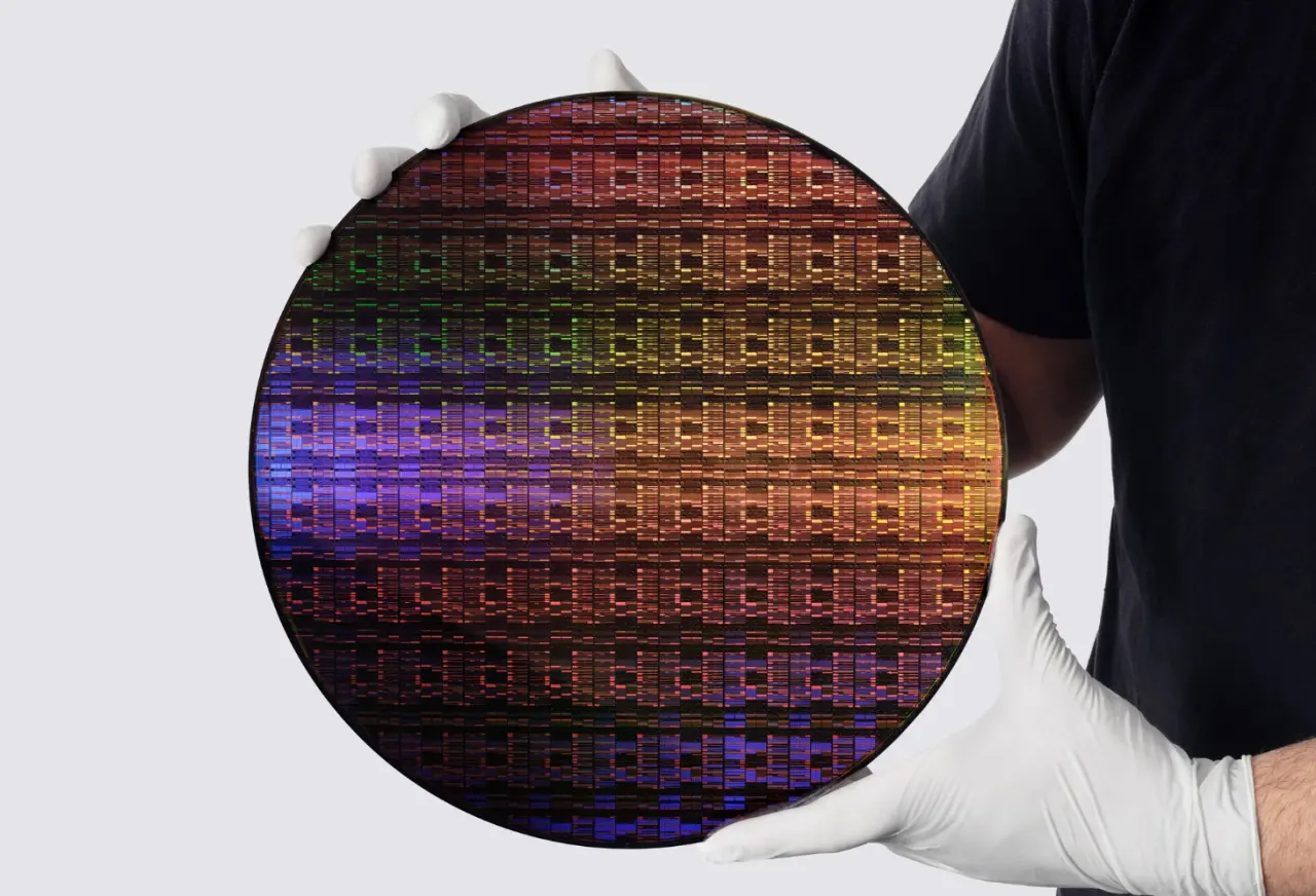
IBM details major chip breakthrough with new sub-1nm ‘nanostack’ 3D architecture
Company claims technology provides up to 50 percent more performance or 70 percent greater energy efficiency
- ·
forbes.com

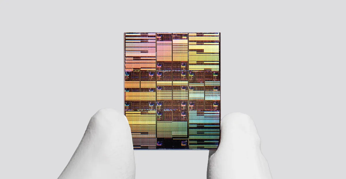
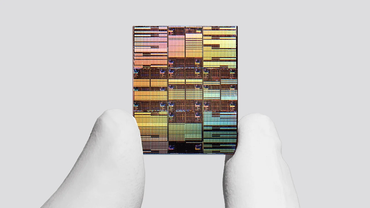
IBM Unveils World’s First Sub-1nm Chip With 100 Billion 3D-Stacked Transistors
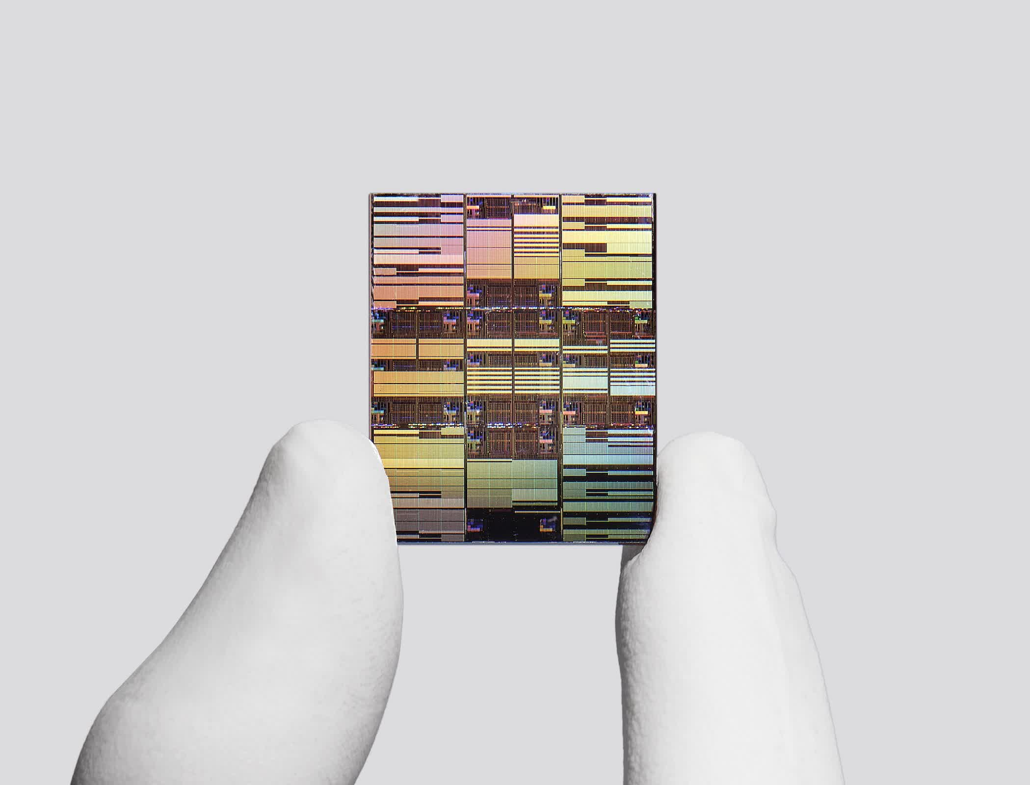
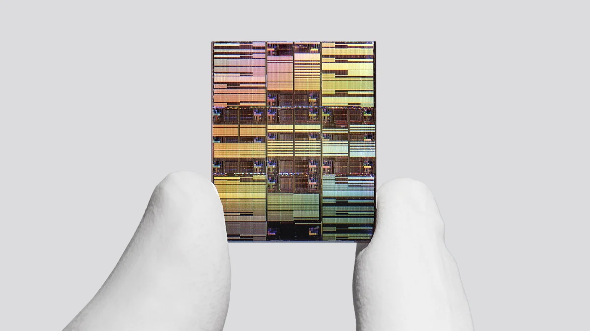
IBM just unveiled the world's first sub 1-nanometer chip: 100 billion transistors. IBM also says they've produced functioning devices with this technology.
- ·
technologyreview.com
IBM has unveiled chip technology that could help extend Moore’s Law another decade
The company, along with others, is pursuing a new paradigm for cramming more transistors on chips—building up.
- ·
research.ibm.com
What is IBM’s nanostack chip architecture?
This new microchip architecture from IBM builds up, not out, to overcome the spatial limitations of scaling transistor density.
- ·
siliconangle.com
IBM says new sub-nanometer architecture paves the way for the next decade of chip design - SiliconANGLE
IBM says new sub-nanometer architecture paves the way for the next decade of chip design - SiliconANGLE
- ·
cryptobriefing.com

IBM proposes NanoStack architecture for ultra-dense 3D chips
IBM's NanoStack architecture promises 50% area scaling and 70% power reduction versus 2 nm chips, targeting next-gen AI accelerators and high-performance
- ·

IBM unveils world's first 0.7nm chip technology with 100 billion transistors
IBM unveiled 0.7nm chip technology with 100 billion transistors using nanostack 3D architecture, projecting 50% more performance or 70% better energy
- ·
spectrum.ieee.org
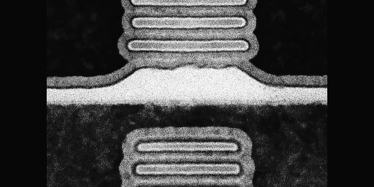
Is This Stacked CFET Architecture The Ultimate CMOS Platform?
IBM chooses a different path from Intel, Samsung, and TSMC
- ·
neowin.net
IBM reveals sub-1nm chip technology, production expected in another 5 years
IBM has just announced a massive breakthrough in semiconductor research: the world's first sub-1-nanometer chip technology.
- ·
theverge.com
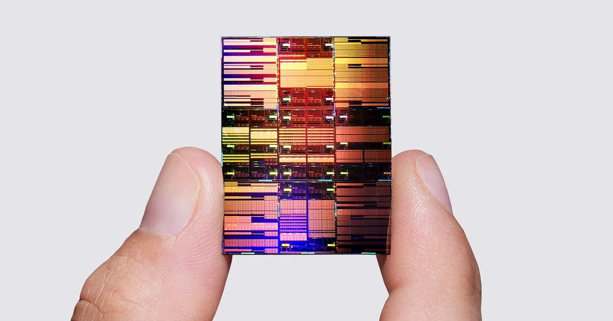
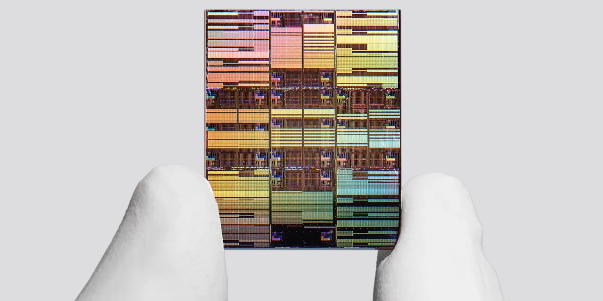
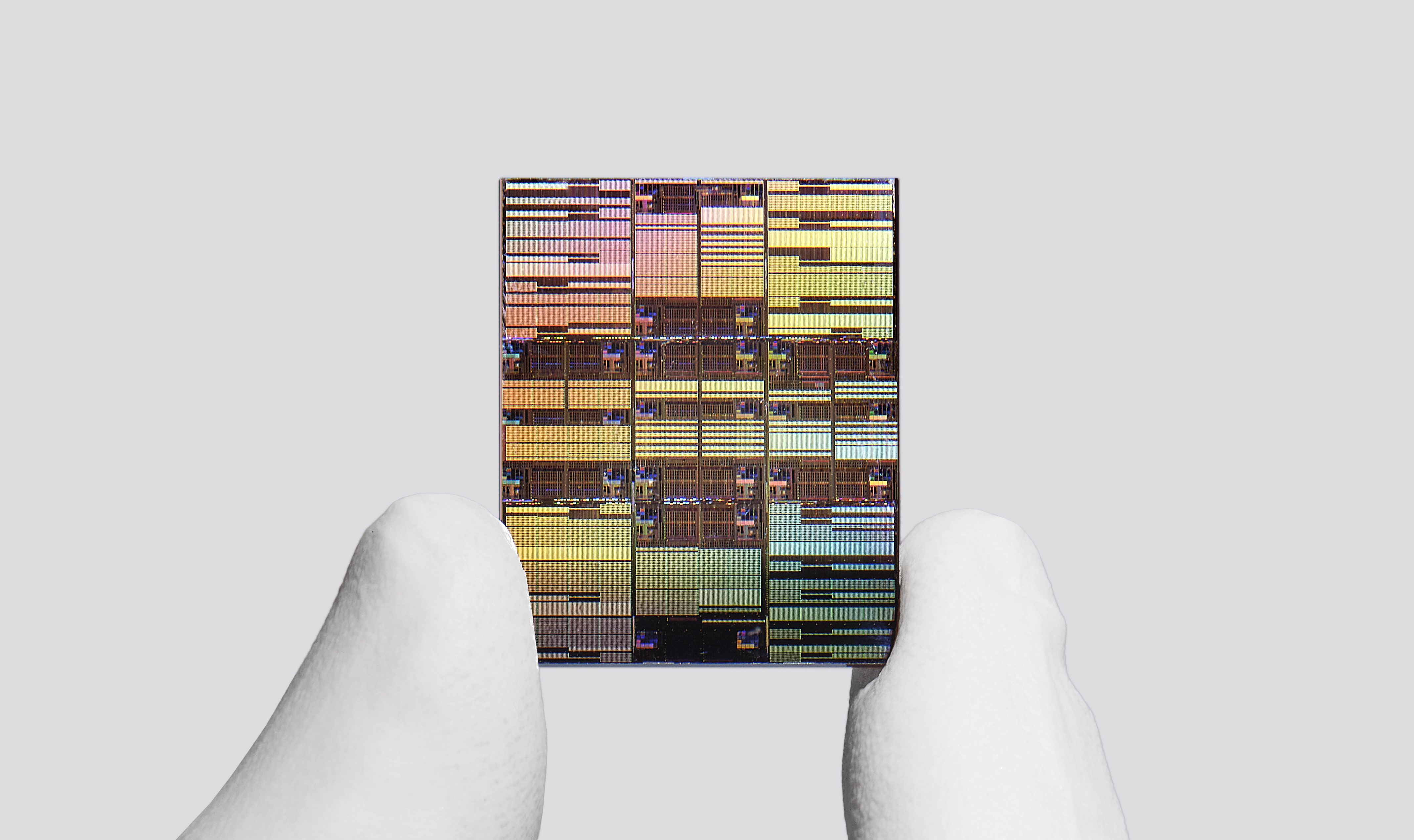
IBM crams 100 billion transistors on a chip the size of a fingernail.
The company claims its new nanostack tech is the first sub-nanometer chip manufacturing process. IBM also says that nanostack can deliver up to 50 percent more performance, or 70…
- ·
news.bitcoin.com
IBM Unveils Sub-1 Nanometer Chip With 100 Billion Transistors, Extending Moore's Law
IBM unveiled the world's first sub-1 nm chip at the 0.7 nm node, packing 100B transistors with 70% better efficiency.
- ·
silicon.co.uk

IBM Unveils 3D-Stacked .7nm Chip Design | Silicon UK Tech News
IBM says 'nanostack' approach could fit nearly 100 billion transistors into fingernail-sized area, amid soaring demand for processing power
- ·
techspot.com
IBM unveils sub-1-nanometer chip architecture that stacks 100 billion transistors onto a fingernail-sized processor
Rather than continuing to shrink components along a flat plane, IBM is stacking transistors vertically. That change comes as semiconductor designers run up against the physical…
- ·
heise.de
0,7 Nanometer: IBM zeigt die ersten Chips mit CFET-Transistoren
IBM zeigt, wie Chips der Zukunft aussehen könnten. Leistung, Effizienz und Transistordichte steigen enorm.