Virtually every high-end GPU and AI accelerator relies on high bandwidth memory (HBM), which can shuffle data around at multiple terabytes a second but can only reach into the gigabytes, with models often needing to be shared across multiple processors. However, an emerging storage technology could change that, boosting accelerator memory capacity from hundreds of gigabytes to terabytes.The technology, called high-bandwidth flash (HBF), is being developed by Sandisk and SK Hynix and aims to provide SSD-like capacities at HBM-like speeds.Peeling back HBF’s layers
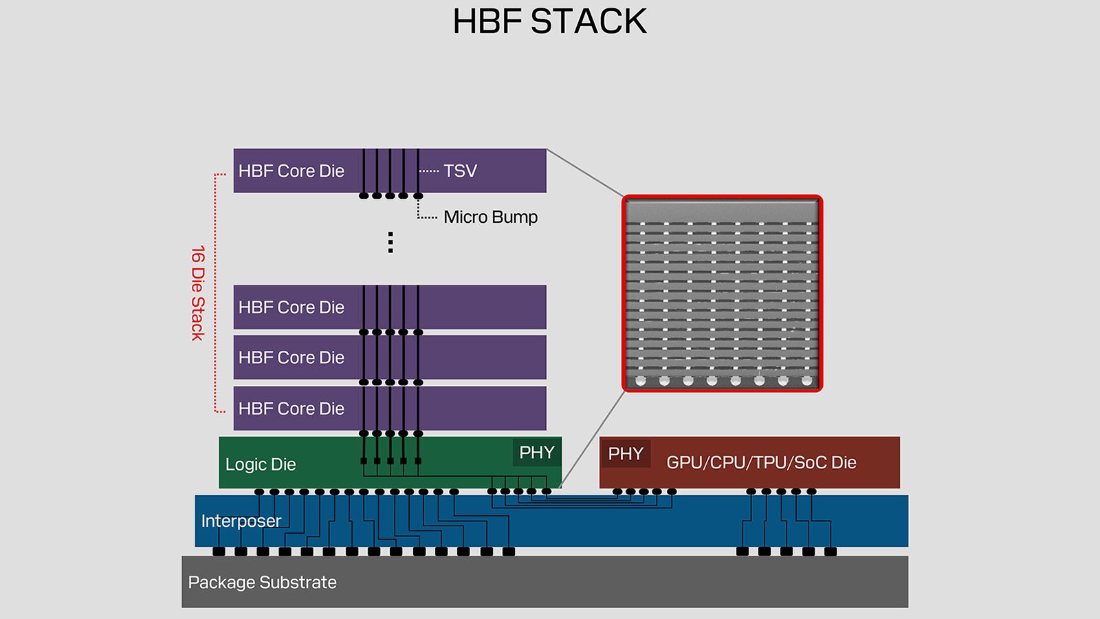
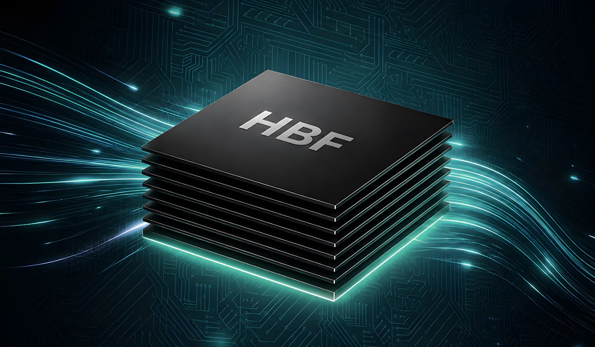
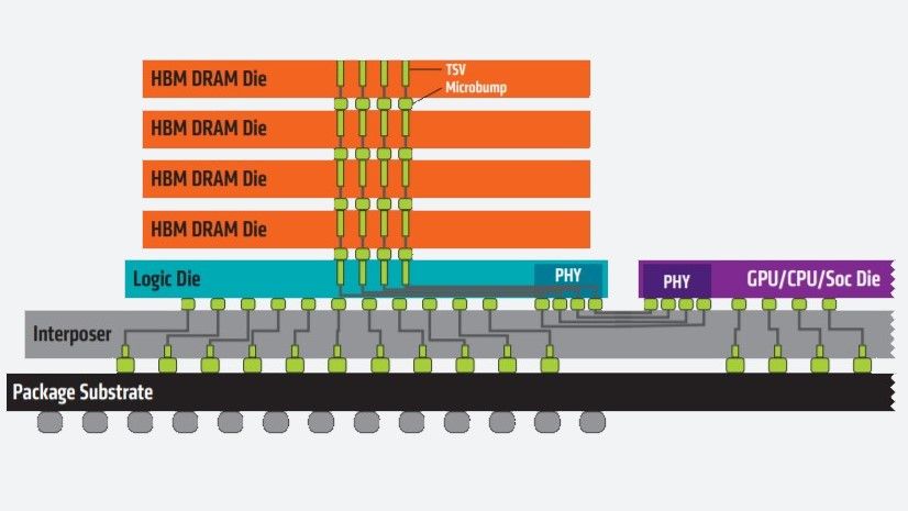
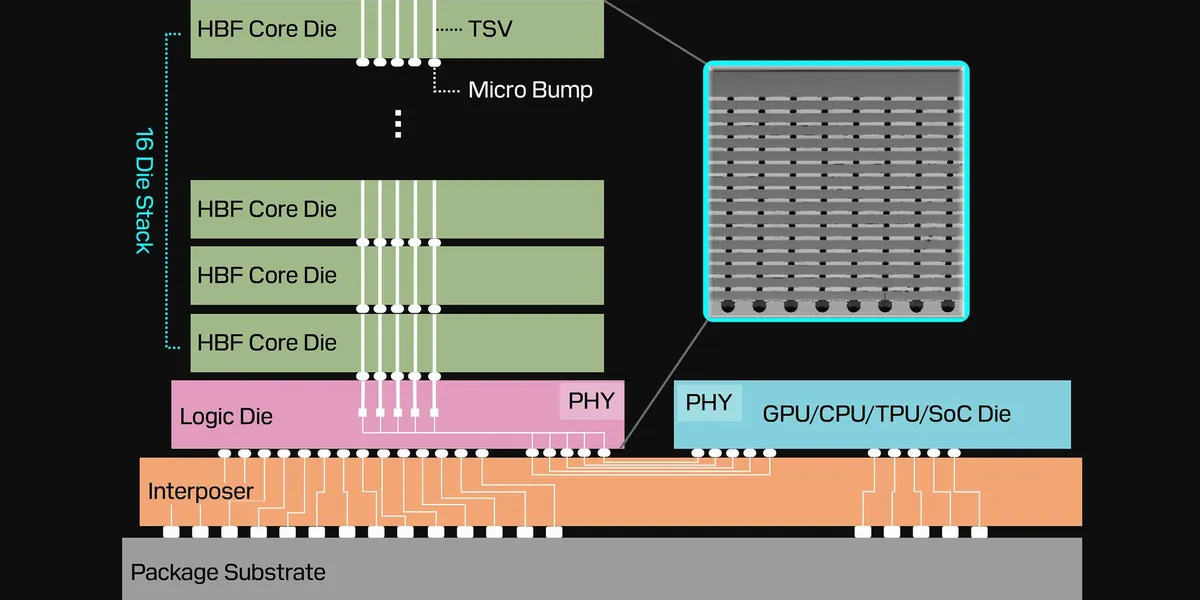
Conceptually, high-bandwidth flash looks and sounds a lot like HBM. It’s assembled by stacking multiple layers (16 in the case of Sandisk’s first-gen modules) of memory together, which boosts capacity and bandwidth. But where HBM uses DRAM, HBF aims to use NAND flash.
Sandisk claims its first generation of high-bandwidth flash will supposedly achieve read bandwidths up to 1.6 TB/s [PDF], making it a bit faster than HBM3e but significantly slower than HBM4, which is already hitting 2.5 TB/s per 12-high stack. Future HBF generations are expected to push bandwidth to over 2 TB/s and eventually 3.2 TB/s.While bandwidth makes HBF interesting as an alternative to HBM, its real party trick is capacity. Because it’s built using NAND, Sandisk says it can achieve capacities up to 256 Gb per die, which translates to 512 GB per 16-high module. That’s more than 14 times the capacity of the HBM4 used in AMD and Nvidia’s latest accelerators.Continuing with the similarities, HBF modules share similar packaging requirements to HBM, which means you can expect them to be fused to the GPU die using advanced packaging techniques like TSMC’s CoWoS, or Intel’s EMIB and Foveros tech. Nothing particularly exotic as AI accelerators go.What’s more, the storage vendor doesn’t expect the modules to come at a power or price premium over HBM. And from a bits per dollar standpoint, HBF looks like a stellar option. If all this sounds a bit too good to be true, that’s because for all of HBF’s benefits, it comes with some rather significant compromises.NAND still isn’t DRAMThe main trade off, as we understand it, is write endurance and access latency. HBF may perform like HBM on paper, but it’s still using NAND, which has a finite write endurance before it wears out and has access latencies measured in microseconds as opposed to tens of nanoseconds for DRAM.If you were to swap HBM for HBF, it (probably) wouldn’t perform very well and it’d wear out pretty quickly, rendering that $50,000-plus GPU of yours a paperweight — not ideal for a product that’s being asked to serve longer to suit hyperscalers' depreciation schedules.