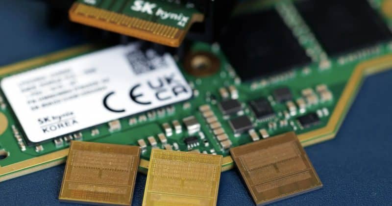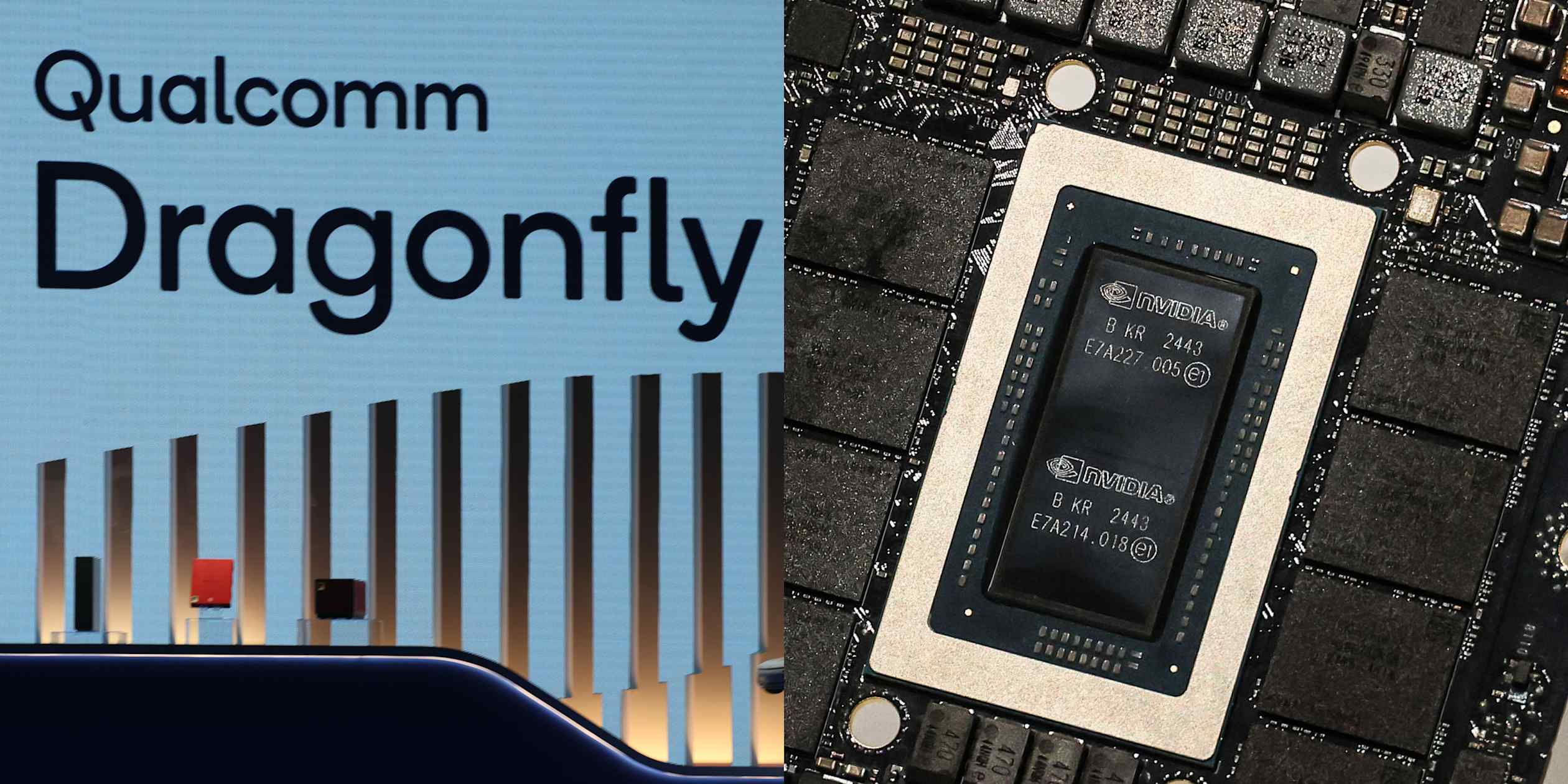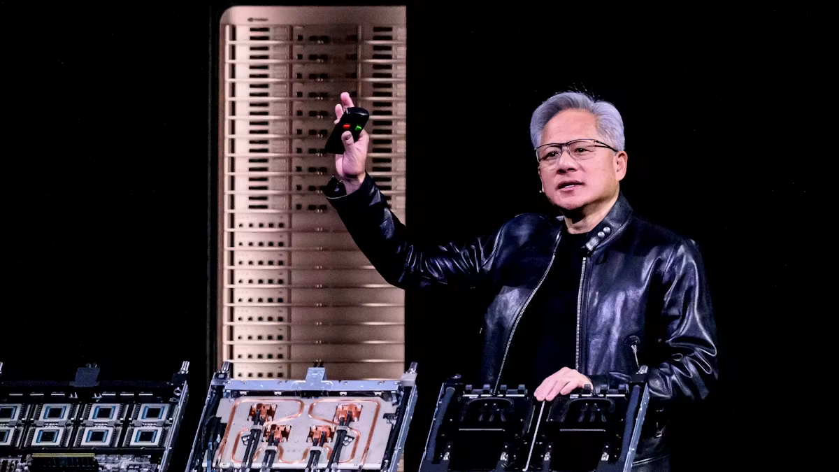
The single most expensive component in a modern AI system is rarely the one people name. It sits a layer beneath the headline silicon, and its scarcity has done more to shape the last two years of the AI build-out than any chip launch. High Bandwidth Memory — HBM — is the fast, stacked, hard-to-manufacture memory bolted alongside every Nvidia accelerator, and it has become the choke point that decides who gets to build AI at scale and who waits in line. Picture the whole data centre as a plumbing system: the compute die is a thirsty engine, and HBM is the fire hose that feeds it — enormous flow, tremendous pressure, and a supply of hoses controlled by a handful of factories straining to make them fast enough.Qualcomm has looked at that fire hose and decided to bring a reservoir instead.That is the wager at the centre of this story, and it is spreading. Qualcomm, Intel, and — in a stranger register — Google are each placing a different bet against the same house. The house is Nvidia, and the chip on the table is the assumption that serving an AI model demands the same memory that training one does. Each challenger is calling that assumption. Each is betting that for inference — the everyday work of a trained model answering real queries — raw capacity, low cost, and low power beat the peak bandwidth that HBM exists to deliver. Whether the bet pays depends on a question the benchmarks have yet to settle. The stakes could hardly be higher, because the pot is the fastest-growing hardware market on earth.Key TakeawaysQualcomm's AI200 accelerator carries 768GB of LPDDR memory per card and skips HBM entirely, holding trillion-parameter models on a single node at a fraction of HBM's cost.At its Investor Day 2026, Qualcomm detailed a near-memory architecture it calls HBC, and named Meta and Microsoft as customers — its first hyperscaler wins.Intel's Crescent Island, detailed at Computex 2026, is effectively the first data-centre GPU built on LPDDR5X rather than HBM, air-cooled and built for inference alone.In an exclusive Computex round table, Intel's Anil Nanduri argued the binding data-centre constraint is shifting from GPU throughput to CPU orchestration — a parallel case against the GPU-only rack.Google and UC San Diego built a working computing cluster from retired Pixel phones, proving the point at its logical extreme: sometimes the cheapest server is one already built.The common thread across all three: inference diverges from training, and the industry over-bought the memory that training needs.The Wall Everyone Is Trying To ClimbStart with why HBM became indispensable, because the answer explains why routing around it is plausible.When a large language model generates text, it does so one token at a time, and that step — the decode phase — has an unusual character. The arithmetic intensity is extremely low: for every byte pulled from memory, very few mathematical operations get performed, so the workload is bounded almost entirely by how fast you can move data, and only lightly by how fast you can compute. In plumbing terms, the engine spends most of its time waiting on the pipe. The industry named this bottleneck the memory wall, and HBM is the answer it settled on — memory dies stacked through silicon interposers in 2. 5D packaging, placed adjacent to the compute die, delivering roughly 3.35 TB/s on Nvidia's H100.The trouble is supply. That stacking process runs through advanced packaging capacity and a memory supply chain concentrated in a few hands, and demand has swamped it. Intel chose an alternative specifically to sidestep the global shortage of high-bandwidth memory, which is controlled by a concentrated supply chain dominated by SK Hynix and Samsung — a supply chain sold out through at least 2027. Every hyperscaler building clusters through 2025 and 2026 has been rationing around the same constraint. So the opening is stark: a company that can serve inference free of HBM sidesteps the tightest bottleneck in AI hardware, and in doing so chips at Nvidia's deepest moat.Qualcomm's Bet: Bring A Reservoir Where Nvidia Brings A HoseQualcomm's data-centre re-entry is the cleanest expression of the idea. Its AI200 accelerator, targeting commercial availability in 2026, carries 768GB of LPDDR memory per card for large-language-model inference. LPDDR is the low-power memory Qualcomm has shipped in phones for fifteen years — slower than HBM, but vastly cheaper and available in volume. That single number is the whole argument: 768GB of LPDDR5X per card is enough to hold models up to 10 trillion parameters on a single node, free of the sharding a GPU cluster forces. Set against the incumbents, it is roughly 10 times the memory of an H100's 80GB and 4.8 times a B200's 192GB.The economics are where the bet gets its teeth. For 768GB of capacity, the memory bill runs roughly $1,500 to $3,000 per card, against $7,600 to $11,500 for the same capacity in HBM3e, a figure so steep that shipping accelerators top out well below it. The reservoir holds far more water than the hose, and costs a fraction to fill. Qualcomm's reasoning is that inference and training drink differently: it is betting that inference workloads exhibit different memory access patterns than training, making capacity more critical than peak bandwidth — an assumption that holds for autoregressive generation, where memory-bound decode dominates.At its Investor Day 2026, Qualcomm named the architecture underneath the roadmap: HBC, or High Bandwidth Compute. Rather than laying memory beside the processor on an interposer, HBC stacks vertically. It places the logic compute die directly beneath a vertical LPDDR memory stack, bonded through dense through-silicon vias. The elegance is in what it dodges: because LPDDR avoids the advanced 2. 5D interposer packaging that HBM demands, Qualcomm sidesteps the CoWoS supply-chain bottleneck entirely. Tony Pialis, who leads Qualcomm's data-centre business, described the move as placing the accelerator directly beneath a DRAM stack, claiming the speed of on-chip memory with the density of stacked capacity. The headline figures Qualcomm attaches: per-watt bandwidth six times that of HBM, and per-watt capacity 200 times that of on-chip SRAM, alongside 4 to 8 times better decode performance per watt.Two facts lift this above a vendor slide. The first is customers. Qualcomm disclosed a multi-generation partnership with Meta, which is adopting its Dragonfly C1000 data-centre CPU — its first formal CPU order from a hyperscaler — and confirmed Microsoft Azure will deploy its HBC chips in the AI250 and AI300 accelerators. When two of the companies designing their own silicon choose to buy yours, the thesis has left the whiteboard. The second is software, historically the graveyard of Nvidia challengers. Qualcomm bought its way toward an answer: the Modular acquisition, an all-stock deal valued at roughly $3.9 billion, supplies a silicon-agnostic layer that schedules work across unlike parts — the piece CUDA has always denied rivals.The roadmap runs on an annual cadence. The AI200 ships on LPDDR5X in late 2026, the AI250 adds HBC Gen 1 in mid-2027, and the AI300 brings HBC Gen 2 in 2028. The bandwidth ramp is steep on paper — the AI250 claims single-card read/write speeds of 133 TB/s, roughly 18 times the AI200, and the AI300 targets up to 54 times. An early anchor deployment is already signed: a partnership with Saudi Arabia's HUMAIN targeting 200 megawatts of AI200 and AI250 racks starting in 2026, each rack liquid-cooled at a 160 kW power envelope, with PCIe for scale-up and Ethernet for scale-out.Intel's Parallel Bet — And What Nanduri Told Me In TaipeiIntel is making structurally the same wager from two directions at once, and the parallel is explicit enough that analysts name it: Qualcomm's approach is a similar bet to Intel's Crescent Island, which also uses LPDDR instead of HBM.Crescent Island, detailed at Computex 2026, is the GPU half of Intel's answer. Built on the Xe3P architecture and described as "built for agentic AI," it forgoes GDDR and HBM memory for LPDDR5X, scaling to up to 480GB of LPDDR5X, with a 160GB reference configuration — a figure that makes it unusual among data-centre GPUs. By most reckonings it is the first AI GPU to use LPDDR5X at all. The physical contrast with Nvidia's approach is deliberate: a 350W power envelope that fits standard air-cooled servers, where HBM systems demand liquid cooling and the infrastructure to run it. Intel has also narrowed its ambition with unusual candour. After the Gaudi accelerator failed to gain traction, Intel stepped back from the training market, with data-centre chief Kevork Kechichian stating plainly that the company will stay out of it. The pitch is inference, where the volume lives. The open risk is the same one that has sunk Intel's accelerators before: its oneAPI software stack remains far less adopted than CUDA or ROCm, and that gap is a real barrier to enterprise uptake. Timeline: customer sampling in the second half of 2026, with meaningful revenue most likely a 2027 story.The CPU half of Intel's argument is where your correspondent had a front-row seat. On the morning of 1 June, in a side room at the Humble House a short walk from the Computex floor, Anil Nanduri — Vice President at Intel leading the AI Acceleration Office, and a company veteran of more than two decades — spent ninety minutes making the case that the data centre's binding constraint is quietly moving off the GPU. As inference turns agentic, Nanduri argued, the work that decides throughput becomes orchestration: the iterative loops, the tool calls, the vector retrieval, the security context, the management of the KV cache that holds a model's working memory. That work runs on the CPU rather than the accelerator, and so, in his telling, the ratio of CPUs to GPUs in a real rack drifts toward parity. The silicon Intel positions for that pattern is Xeon 6+ on the 18A node, carrying up to 288 efficient cores, a twelve-channel DDR5 memory subsystem, and 96 lanes of PCIe Gen 5 with CXL.The sharpest evidence Nanduri offered came from a customer's ledger rather than an architecture diagram. Pairing Xeon with the Arc Pro B70 workstation GPU — 32GB of memory per card, four cards to a workstation — a hybrid stack can run a 120-billion-parameter model locally and keep roughly 80 per cent of an agentic workload on the desk, sending only the premium queries to the cloud. He described one customer whose cloud-token bill of $3,000 a month paid off a workstation of about $5,000 inside two months. And the phrase he kept returning to, the one that framed the whole conversation, was a measure of waste: twenty watts. That is roughly what the human brain runs on, against the megawatts a data centre burns to chase the same reasoning — three orders of magnitude, still unclosed. It is the same accusation Qualcomm's memory argument makes in a different accent: the industry has been paying, at ruinous scale, for the wrong resource.Google's Radical Version: A Server Made Of Dead PhonesGoogle's contribution takes the same instinct — question what a data centre must be built from — and pushes it past the point of provocation. Published on 12 June 2026 with the University of California San Diego, the project is called phone cluster computing, and the method reads like a thought experiment made real. Retired Pixel smartphones are stripped of everything unnecessary for computing — displays, batteries, cameras, speakers, casings — leaving only the motherboard with its system-on-chip, which in recent Pixels is Google's own Tensor processor. Android is replaced with a general-purpose Linux distribution, and the bare boards are bound into self-managing clusters using Kubernetes.The surprise is that the phones hold their own. Smartphones released roughly three years ago can still outperform certain server configurations on a single-core basis in SPEC benchmarks — concretely, a 2023 Pixel Fold beats the per-core performance of a baseline dual-socket server running two AMD EPYC processors on most benchmarks. Stacked up, the maths turns practical: roughly 25 to 50 phones match the compute output of a single dual-socket server, and a cluster of 20 phones already serves an application for a class of more than 75 students with latency below comparable cloud backends. The plan scales that up hard — a 2,000-Pixel cluster, expected to go live ahead of the academic year, capable of supporting a hundred computer-science courses at once.The motive braids sustainability with the same cost pressure squeezing the chip makers. Manufacturing the chip and board accounts for roughly half of a smartphone's entire lifetime carbon footprint, so extending a phone's life as a server avoids that embodied cost outright — and it lands as memory and storage prices keep climbing, which sharpens the "fraction of the usual cost" argument. Two caveats keep it honest. The project is aimed at the modest workloads universities already run rather than at GPU clusters for training frontier models. And the idea has form: NASA repurposed a Qualcomm Snapdragon 801 to help the Perseverance rover and Ingenuity helicopter navigate on Mars. Google's own version simply proves the outer edge of the same thesis — that for a large class of real work, the cheapest, greenest server is one that has already been built.The Through-Line: Inference Diverges From TrainingSet the three bets side by side and the shared logic sharpens. Nvidia's dominance rests on HBM bandwidth tuned for the training run, the event that happens once. The cost that recurs forever is decode-heavy inference, where the binding constraints are capacity, power, and price. Qualcomm attacks it with LPDDR capacity and near-memory HBC. Intel attacks it with LPDDR5X GPUs and a CPU-orchestration thesis Nanduri laid out in person. Google attacks it by refusing to manufacture new hardware at all. Three accents, one argument: the industry over-bought the memory that training needs, and inference can be served on something cheaper.The betting metaphor holds because the challengers claim better pot odds than Nvidia rather than a better hand. Every one of these products trails a Blackwell on peak throughput, and each concedes as much. What each offers is more model per dollar, per watt, per rack, for the workload that now dominates the meter. Even the market's reflex agreed: Qualcomm's data-centre announcement added roughly $20 billion to its market value on the day, and the company forecasts a global AI accelerator market reaching $680 billion by fiscal 2029. A modest share of a pot that size rewrites a balance sheet.The Skeptic's View An honest read has to deal Nvidia's cards too, because the counter-argument is real. Bandwidth is a genuine limit in inference, and LPDDR trades it away. The unresolved question hangs over every one of these bets: the TCO maths only works if a deployment avoids needing 2 to 6 times more racks than an equivalent GPU system to match throughput. Cheap memory saves money only when it feeds the engine fast enough to matter.Qualcomm's HBC carries a second risk, one Nvidia has named out loud. Nvidia has publicly acknowledged that stacking DRAM directly on logic at scale requires advances in materials science and intra-chip cooling that remain out of reach at production volumes — because burying the processor under heat-sensitive memory invites a thermal feedback loop that degrades the very bandwidth the design chases. Qualcomm's answer is that inference avoids the sustained thermal load of training, and that its racks are built for direct liquid cooling at 140 to 160 kW envelopes. That claim, like the throughput claims, awaits independent benchmarks — and for both Qualcomm and Intel, the products that matter most arrive in 2027 and 2028, an eternity in this market. The software gap remains the quiet killer: an ecosystem takes years to mature, and CUDA has a decade's head start.The India ContextFor the Indian data-centre build-out, the economics land close to home. India is adding capacity fast, and the constraints that bite hardest here are power and cooling cost — precisely the axes on which the anti-HBM camp competes. An air-cooled inference accelerator that fits an existing rack, draws less power, and skips the liquid-cooling retrofit maps onto the balance sheet of an operator building in a market where energy is the dominant line item. The HBM shortage is global, but its relief for a cost-sensitive deployment could arrive first through exactly this class of hardware. For the enterprises weighing where to run their models, the arrival of credible options beyond a single, scarce, expensive supplier is the shift that matters — and it is arriving from three directions at once.Nvidia remains the default, and will for years. What changed in the space of a Computex keynote and an Investor Day is that the default now has company. The memory wall still stands. For the first time in a while, more than one company is convinced it can be walked around — and two of the biggest buyers in the world have started to agree.FAQWhy is Qualcomm avoiding HBM in its data-centre chips?HBM is expensive, scarce, and hard to manufacture, with supply sold out to 2027. Qualcomm uses LPDDR memory instead, which is cheaper and available in volume, betting that AI inference needs memory capacity more than the peak bandwidth HBM provides. Its AI200 card carries 768GB of LPDDR at a fraction of HBM's cost.What is Qualcomm's HBC architecture?HBC, or High Bandwidth Compute, is Qualcomm's near-memory design that stacks the compute die directly beneath a vertical LPDDR memory stack, connected by through-silicon vias. Because LPDDR skips the advanced packaging HBM requires, HBC sidesteps the CoWoS supply-chain bottleneck. Qualcomm claims six times the bandwidth per watt of HBM.How is Intel's Crescent Island similar to Qualcomm's approach?Both skip HBM for cheaper LPDDR memory aimed at AI inference. Intel's Crescent Island, detailed at Computex 2026, uses up to 480GB of LPDDR5X, runs air-cooled at 350W, and is built for inference rather than training. Analysts describe it as the same bet Qualcomm is making.What did Intel's Anil Nanduri argue about CPUs and AI?In an exclusive Computex 2026 round table, Nanduri argued that agentic AI shifts the binding data-centre constraint from GPU throughput to CPU orchestration, memory access, and software flexibility. He positioned Intel's Xeon 6+ on the 18A node for that workload and cited a customer whose cloud bill paid off a local AI workstation in two months.What is Google's phone cluster computing project?Google and UC San Diego built a computing cluster from retired Pixel smartphones, stripping them to the motherboard, replacing Android with Linux, and linking them with Kubernetes. A 2,000-phone cluster is planned to support around 100 university courses. It targets modest university workloads rather than frontier AI training.Does skipping HBM mean these chips beat Nvidia?On raw throughput, Nvidia's top accelerators stay ahead. These products trade peak bandwidth for capacity, cost, and power efficiency instead. Their case is lower total cost of ownership for inference. The unresolved question is whether lower bandwidth forces enough extra racks to erode that saving.When do these chips arrive?Qualcomm's AI200 ships in late 2026, the AI250 in mid-2027, and the AI300 in 2028. Intel's Crescent Island samples to customers in the second half of 2026, with revenue likely in 2027. Google's phone cluster is a research deployment expected to go live ahead of the coming academic year.end of article
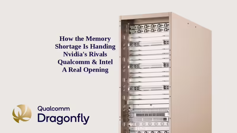
How the Memory Shortage Is Handing Nvidia's Rivals Qualcomm & Intel A Real Opening
The memory that made Nvidia untouchable is scarce, expensive, and sold out to 2027. Qualcomm, Intel, and Google are each betting they can route around it. Qualcomm packs 768GB of cheap mobile memory onto a single inference card, Intel builds the first data-centre GPU that skips HBM altogether, and Google turns dead Pixels into a server. Three bets, one target: the memory tax that underwrites Nvidia's lead.
3,191 words~15 min read