Qualcomm is finally getting serious about AI infrastructure, but its push into the datacenter hinges on the success of an ambitious near-memory compute architecture designed to deliver better inference economics than today's GPUs.Announced during its 2026 investor day last week, the tech will see Qualcomm stack layer upon layer of DRAM on top of its XPUs to form a single unified compute and memory module it's calling high-bandwidth compute (HBC).“We offer all of the performance advantages of SRAM, but with the density and the memory capacity that HBM (high-bandwidth memory) stacks offer,” Tony Pialis, Qualcomm’s EVP of datacenter, claimed during last week's investor presentation.
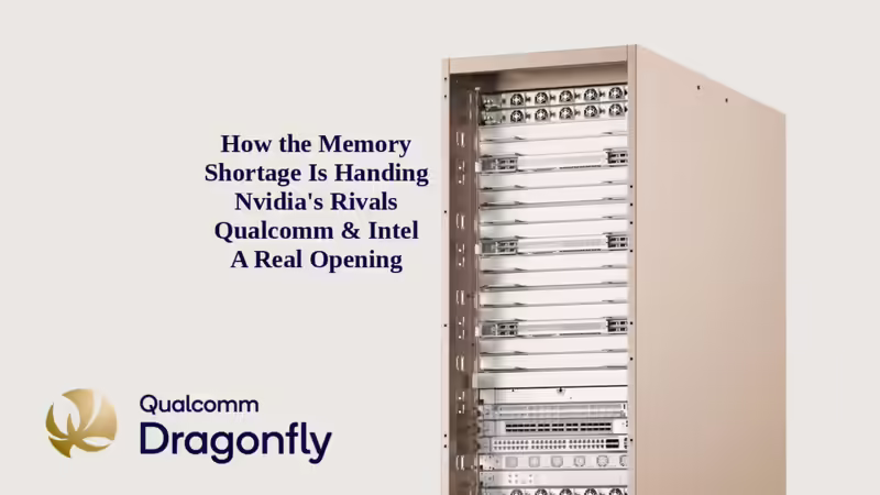
This technology is set to launch next year as part of Qualcomm’s AI250-series of Dragonfly rack systems, and marks a distinct shift in Qualcomm’s AI infrastructure strategy. The handset giant is no stranger to AI accelerators. Essentially every Snapdragon processor sold today ships with an NPU on board. But in the datacenter, the company has struggled to garner the same excitement as Nvidia, AMD, and even startups like Cerebras.
Compared to the big two’s GPUs, Qualcomm’s AI-series accelerators haven’t compared that favorably, but that could soon change as the company looks to make its mark on the datacenter.With the AI250, the SoC maker is claiming 768 GB of memory capacity and up to 133 TB/s of effective memory bandwidth per card. For reference, Nvidia's Groq 3 LPUs offer just 500 MB of SRAM and 150 TB/s of bandwidth.If that seems too good to be true, that’s because it is. Qualcomm is leaning heavily on the word “effective.” We know that because for the AI200-based Dragonfly systems rolling out this year, they claimed 414 TB/s of “effective” memory bandwidth across all 56 chips. On its face, that seems more realistic, but actually achieving that with 8800 MT/s LPDDR5x alone would require a 6,720-bit-wide bus, which it almost certainly does not possess. Qualcomm insists that this is the "pure physical bandwidth of the LPDDR interface," but declined to offer any specifics as to how it's somehow managed to achieve what Nvidia needed eight HBM3e stacks to do.In any case, according to Qualcomm’s marketing materials, with the move to HBC, the AI250 will offer 18x the effective bandwidth of the AI200, while the forthcoming AI300 will deliver 54x the bandwidth. Given the context, these seem like outlandish claims, but these "effective" multipliers are really a feature of Qualcomm's HBC architecture.Unpacking high-bandwidth computeAmplifying “effective” bandwidth isn’t the only party trick from these HBC-based accelerators. Qualcomm claims that by moving some of the XPU’s compute under the DRAM, it can significantly reduce the amount of power its chips consume.On a conventional datacenter GPU, data is rapidly shuffled between HBM and the compute dies. Even using advanced packaging technologies like TSMC’s CoWoS, the power required to move this data back and forth is significant.