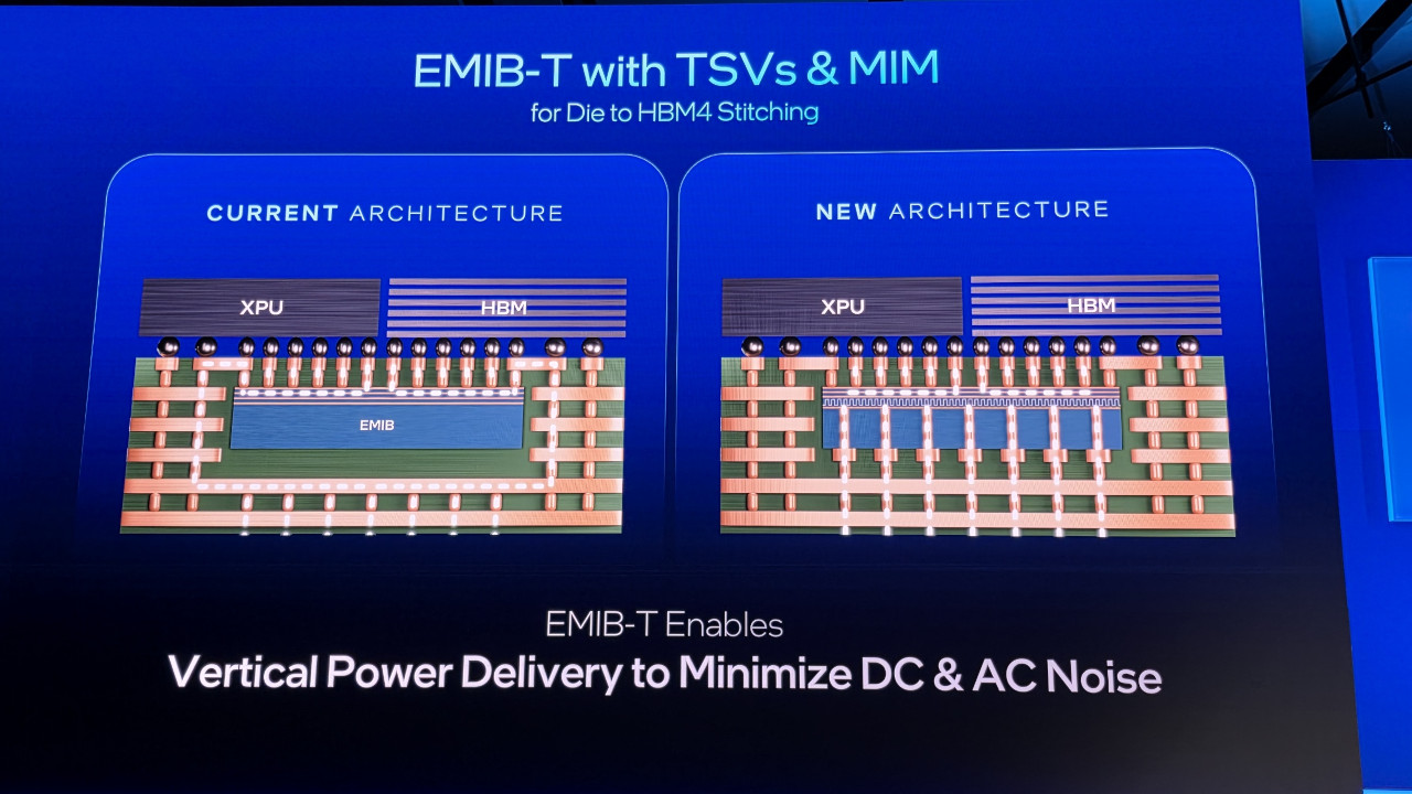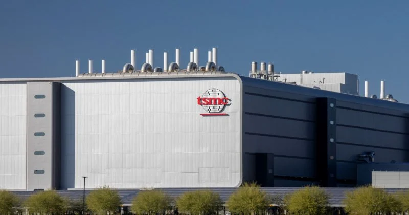
TSMC is building a new type of chip packaging technology called CoPoS, short for Chip-on-Panel-on-Substrate, that swaps traditional circular wafers for larger rectangular panels. The move is designed to squeeze more usable area out of each production run and directly challenge Intel’s competing EMIB platform in the race to package ever-larger AI processors.
From circles to rectangles
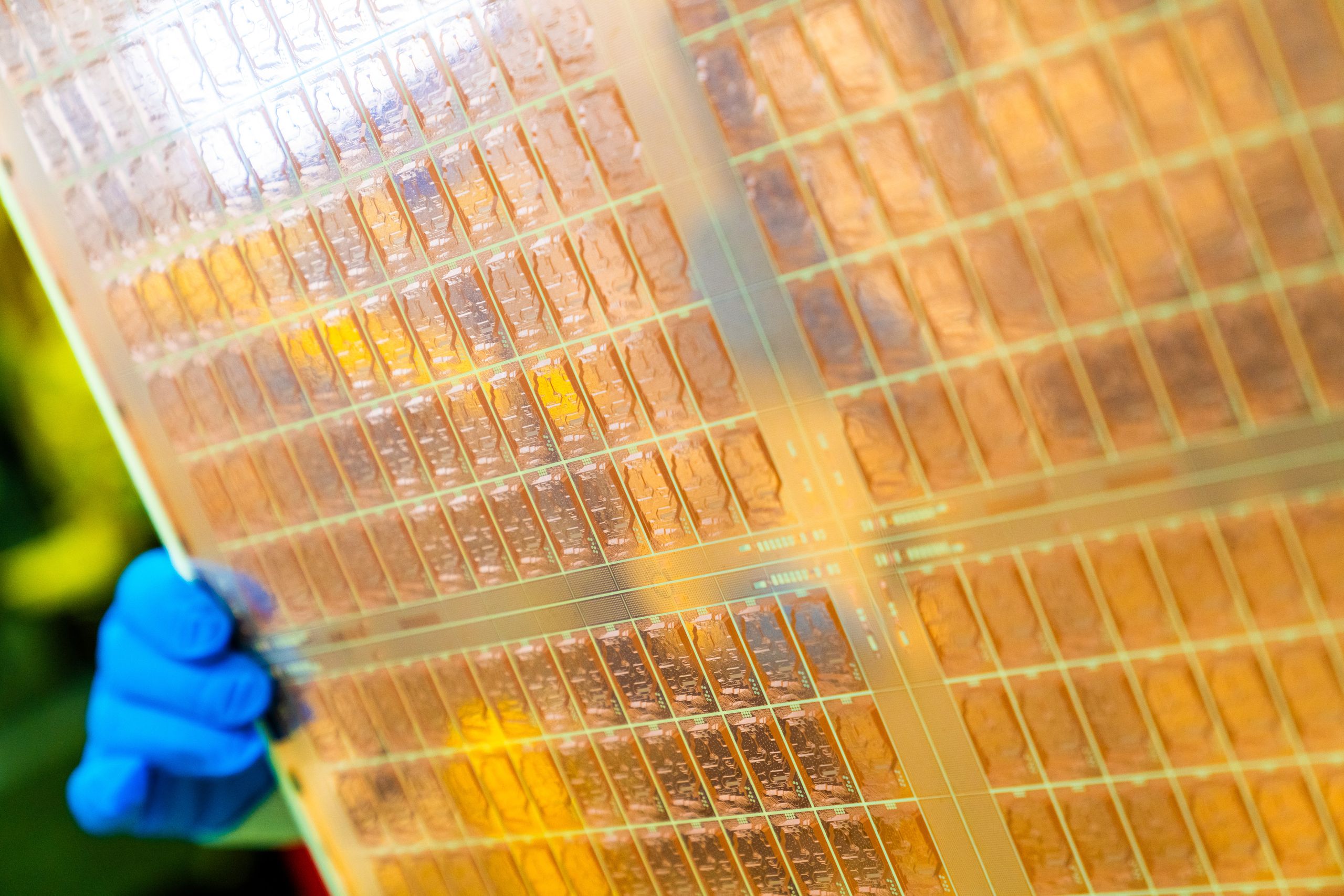
The core innovation is deceptively simple. Traditional semiconductor packaging uses circular 300mm wafers, which waste material around the edges because chips are square. TSMC’s CoPoS technology starts with rectangular panels measuring 310×310 mm, dramatically increasing the usable surface area per production unit.
TSMC’s current advanced packaging platform, called CoWoS (Chip-on-Wafer-on-Substrate), has been the gold standard for high-performance AI chips. Nvidia’s data center GPUs rely on it heavily. The problem is that CoWoS capacity is fully booked through 2027, creating a bottleneck that limits how quickly the AI industry can scale.
CoPoS is the relief valve. Pilot production reportedly commenced around June 2026 at VisEra’s Longtan plant in Taiwan, with mass production not expected until the second half of 2028 or possibly into 2029. TSMC is also exploring glass substrates for the technology, which could improve both performance and cost efficiency compared to conventional organic substrates.