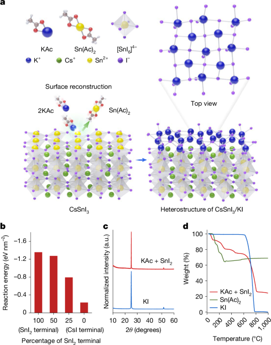
MainTin (Sn2+) halide perovskites have emerged as a model platform for exploring defect-tolerant, lead-free semiconductors that combine electronic functionality with chemical tunability5. Their soft and polarizable lattice and low effective mass enable efficient charge transport, and they can be used to fabricate high-performance optoelectronic devices, including solar cells, light-emitting diodes and thin-film transistors (TFTs)6,7,8,9,10,11. Beyond device performance, these materials provide a unique opportunity to study metastable semiconductor systems, in which an apparent defect tolerance coexists with intrinsic redox activity12,13,14,15. However, this coexistence also introduces a fundamental limitation: the same chemical softness that enables high electronic performance simultaneously destabilizes the electronic ground state.In Sn2+ perovskites, this instability manifests as spontaneous self-p-doping and rapid degradation driven by redox-active defects and highly reactive undercoordinated surface Sn sites16,17. As a result, precise control over the carrier density and threshold voltage remains challenging, which limits their integration into reliable electronic devices. Existing strategies, including additive engineering, dimensional modulation and crystallinity control, have achieved partial stabilization but often at the expense of carrier transport, while largely overlooking the dominant role of surface defect chemistry18,19,20. This leads to a central challenge for Sn-based perovskites: how can we establish a chemically and electronically equilibrated state that simultaneously suppresses self-doping and enables stable device operation.Here we introduce a volatile-assisted coordination strategy to regulate surface defect chemistry and self-doping in Sn2+ halide perovskites. Acetate vapour transiently coordinates with undercoordinated Sn sites and volatilizes upon mild annealing. This drives a spontaneous surface reconstruction that transforms reactive SnI2-terminated surfaces into chemically stabilized, defect-mitigated interfaces. This reconstruction suppresses self-doping and stabilizes the perovskite channel, which enables the fabrication of p-channel transistors with robust and controllable transport characteristics. More importantly, the reconstructed interface acts as a self-passivating and thermally resilient barrier, leading to markedly enhanced ambient and thermal stability, with devices maintaining stable operation for over 1 month at 100 °C. These results establish volatile-assisted surface reconstruction as an effective route for defect equilibration in metastable semiconductors, and they provide a general strategy for enabling stable, device-grade functionality in Sn2+-based materials.Volatile-surface reconstructionTo elucidate the origin of metastability in Sn2+ halide perovskites, we investigated how surface chemistry dictates their structural and electronic degradation. The predominant instabilities arise from surface-localized defects, such as tin vacancies (VSn) and undercoordinated Sn2+ terminals, which form both intrinsically during crystallization and upon exposure to trace oxygen21. The formation energies of these point defects follow this order: surface (0.11 eV), grain boundaries (0.43 eV) then bulk (1.01 eV), which underscores the strong thermodynamic preference for defect generation at surfaces22,23,24. The exact surface termination plays a decisive role in this process: Sn2+ halide perovskites typically expose two types of terminations, AX (for example, CsI) and BX2 (for example, SnI2). Among them, SnI2-terminated surfaces are chemically unstable and highly reactive, and they have larger formation energies than their CsI counterparts (Supplementary Fig. 1). The exposed, undercoordinated Sn2+ atoms at these SnI2 terminals readily oxidize or form VSn, leading to elevated hole concentrations and accelerated structural degradation25,26,27. These reactive sites act as dominant centres for charge-trapping, scattering and irreversible performance loss17,28. By contrast, AX-terminated surfaces are intrinsically more stable, as Sn2+ ions are shielded within the A-site cation halide framework3,29.To chemically reconstruct the reactive SnI2-terminated surfaces, a thin layer of potassium acetate (KAc) was introduced onto a perovskite film. Unlike previous strategies with KAc or potassium iodide (KI), which mainly rely on buried-interface passivation, bulk defect compensation or crystallization control in photovoltaic systems30,31,32, the present approach operates through a volatile, surface-selective reconstruction pathway that directly re-equilibrates the defect chemistry of metastable Sn2+ halide perovskite transistor channels. The acetate anions can transiently coordinate with undercoordinated Sn2+ species, thus initiating a substitution reaction that replaces surface Sn with K and concurrently forms KI. The reaction is as follows: SnI2 (surface) + 2KAc → 2KI + tin (II) acetate (Sn(Ac)2)↑. During this process, the unstable SnI2 terminations are removed, and the volatile by-product Sn(Ac)2 desorbs upon mild annealing (approximately 100 °C), thus yielding a self-limited KI-rich surface-reconstructed CsSnI3 structure (Fig. 1a). Density functional theory calculations revealed that KI anchoring at the CsSnI3 surface lowers the total energy, whereas the acetate-driven substitution is energetically favourable, being strongly exothermic with a calculated enthalpy of approximately −1.4 eV nm−2 at full SnI2 coverage, which confirms that the reaction preferentially occurs at SnI2-terminated surfaces (Fig. 1b). The surface reconstruction preserves the intrinsic hole-transport characteristics of CsSnI3 because the resulting KI has a wide bandgap and electronically inert character (Supplementary Fig. 2).Fig. 1: Mechanism of KAc-driven surface reconstruction.a, Schematic illustration of the volatile-surface reaction. KAc selectively etches reactive SnI2 terminations on CsSnI3 and forms a stable KI passivation layer. b, Calculated reaction enthalpy for the surface substitution reaction (SnI2 + 2KAc → 2KI + Sn(Ac)2) as a function of SnI2 surface coverage. c, XRD patterns of SnI2:KAc mixtures and reference KI films, confirming KI formation after the reaction. d, Thermogravimetric analysis curves of SnI2:KAc mixture, Sn(Ac)2 and KI powders, showing early mass loss of SnI2:KAc due to volatilization of Sn(Ac)2. a.u., arbitrary units.Experimental evidence corroborated the proposed reaction pathway. X-ray diffraction (XRD) of the SnI2:KAc reaction product shows a distinct peak at 25.06°, which is assignable to KI (Fig. 1c and Supplementary Fig. 3). Transmission electron microscopy of the surface-reaction model system of the SnI2 and KAc reaction revealed a uniform cubic lattice with an interplanar spacing of 3.58 Å, in close agreement with the 3.62 Å d-spacing of the reference KI film (Supplementary Fig. 4) and with the KI reflection at 25.06° in the XRD pattern (Fig. 1c). A thermogravimetric analysis confirmed the exothermic nature of the conversion process, as the SnI2:KAc mixture showed an early mass loss near 60 °C, which is well below the vaporization temperature of pure Sn(Ac)2 (approximately 100 °C). The heat released lowered the activation barrier for Sn(Ac)2 and accelerated volatilization (Fig. 1d). This is supported by X-ray photoelectron spectroscopy (XPS), which found that the C 1s peak at 288.5 eV (C=O) in KAc-treated CsSnI3 films disappeared completely after 100 °C annealing33,34 (Supplementary Fig. 5). Furthermore, time-of-flight secondary-ion mass spectrometry and Fourier-transform infrared spectra confirmed the thermal removal of the Sn acetate species. Following post-annealing at 100 °C, the initial surface-concentrated CH3COO− signal became negligible, and the characteristic CH3COO− coordination band at approximately 1,615 cm−1 also vanished35,36 (Supplementary Figs. 6 and 7). By contrast, the KI phase remained thermally stable up to approximately 600 °C. It formed a robust capping layer that effectively protected the underlying perovskite channel and mitigated its intrinsic thermal and ambient instability (Fig. 1d).KAc-treated CsSnI3 film characteristicsTo elucidate how KAc treatment reconstructs the surface and electronic structure of an Sn2+ perovskite film, the structural, chemical and electronic properties of pristine and KAc-treated films were systematically examined. The pristine CsSnI3 film (prepared with PbCl2 incorporation following our established protocol37) served as a reference. XRD patterns of both films exhibited the characteristic orthorhombic β-γ CsSnI3 reflections at (101) and (202), which confirmed that the KAc treatment had not altered the bulk crystal structure (Fig. 2a). By contrast, a distinct diffraction peak near 25° emerged in the KAc-treated film, which evidenced the formation of a detectable KI phase.Fig. 2: Structural and surface characterization of pristine and KAc-treated CsSnI3 films.a, XRD patterns showing identical orthorhombic CsSnI3 reflections and the emergence of a weak diffraction feature (*) associated with KI formation. b, Sn 3d5/2 XPS spectra revealing reduced fractions of undercoordinated Snδ<2+ and Sn4+ after KAc treatment. c, Photoluminescence spectra displaying the enhanced emission intensity of the KAc-treated film, indicative of suppressed non-radiative recombination. d, SEM images showing the comparable grain morphology. e, Atomic force microscopy images showing the surface roughness. f, Kelvin probe force microscopy potential map and corresponding graph extracted over the scan range indicated by the red dashed line, which reveal the higher surface potential of the KAc-treated region, thus confirming the reduced work function and mitigated self-p-doping. r.m.s., root mean square. Scale bars, 1 µm (d,e), 10 µm (f).XPS revealed pronounced surface reconstruction induced by KAc. The fraction of undercoordinated Snδ<2+ species decreased from 11.2% to 1.7% and that of oxidized Sn4+ from 8.3% to 4.3% after treatment (Fig. 2b). These reductions align with the proposed volatile-surface pathway, and they indicate that KAc effectively removed reactive SnI2 terminals and suppressed Sn2+ oxidation, thereby equilibrating the Sn valence distribution. Optical measurements support this conclusion: the photoluminescence intensity increased markedly after treatment, which indicates that there was reduced non-radiative recombination due to defect elimination (Fig. 2c). Time-resolved photoluminescence showed a corresponding increase in carrier lifetime from 20 ps to 90 ps (Supplementary Fig. 8), confirming the suppressed trap-assisted decay and improved surface passivation.Scanning electron microscopy (SEM) showed that both pristine and KAc-treated films had uniform grains without visible pinholes or aggregation (Fig. 2d). A larger-scale SEM image and a corresponding statistical analysis of the grain-size distribution of 3.49 ± 1.26 μm confirm the uniformity of the vapour-deposited CsSnI3 film (Supplementary Fig. 9). Atomic force microscopy found comparable surface roughness levels, with root-mean-square values of approximately 10 nm (Fig. 2e). These observations indicate that the surface reaction proceeded uniformly without altering the film morphology. The time-of-flight secondary-ion mass spectrometry characterization found uniform surface coverage without localized aggregation, as evidenced by a laterally homogeneous K+ signal. Depth profiling confirmed that this surface-reconstructed, KI-rich passivating layer was strongly confined to the top approximately 10 nm of the KAc-treated film (Supplementary Fig. 10). Kelvin probe force microscopy then provided direct evidence of the electronic modulation: KAc-treated regions had a higher surface potential relative to pristine CsSnI3 (Fig. 2f), corresponding to a reduced work function and alleviated self-p-doping. The upward shift of the Fermi level is consistent with the elimination of hole-inducing Sn vacancies and associated trap states at the film surface38,39.To differentiate chemical reconstruction from simple physical deposition, control experiments were performed by directly evaporating KI onto CsSnI3. SEM images revealed discontinuous, island-like KI clusters rather than conformal coverage (Supplementary Fig. 11), and both photoluminescence and time-resolved photoluminescence spectra showed that there was negligible improvement relative to pristine CsSnI3 (Supplementary Fig. 12). This aggregation arose from the lattice mismatch and high interfacial energy between KI and CsSnI3, which favoured Volmer–Weber island growth to minimize the surface free energy. By contrast, KAc treatment drove an in situ substitution reaction that occurred preferentially at undercoordinated SnI2 sites. The exothermic nature of this reaction thermodynamically promoted uniform KI formation directly at the reactive surface to yield a self-limited, conformal and strongly bonded passivation layer. Thus, the observed electronic reconstruction due to the suppression of surface defects originated from the volatile-acetate-mediated chemical process rather than physical KI deposition.Performance of KAc-treated CsSnI3 TFTsThe impact of KAc-induced surface reconstruction on device performance was evaluated using bottom-gate, bottom-contact TFTs (Fig. 3a). Pristine CsSnI3 TFTs exhibited typical p-type depletion-mode behaviour, with a large threshold voltage VTH = 29.5 V, a hole mobility μFE of approximately 30 cm2 V−1 s−1, an on/off current ratio Ion/Ioff of approximately 107 and a subthreshold swing of 0.93 V dec−1. After KAc treatment, the transistors showed markedly improved and more controllable operation, including a reduced VTH of 5 V, Ion/Ioff > 108, a lower subthreshold swing of 0.49 V dec−1 and reduced hysteresis (Fig. 3b and Supplementary Fig. 13). Notably, these improvements were achieved without degrading the on-state current, indicating that the volatile-assisted surface reconstruction effectively regulated charge neutrality while preserving transport.Fig. 3: Electrical characteristics of pristine and KAc-treated CsSnI3 TFTs.a, Schematic of the bottom-gate, bottom-contact TFT architecture. b, Transfer curves of pristine and optimized KAc-treated devices showing improved device characteristics. IG is the gate leakage current. IDS is the drain current. VGS is the gate voltage. c, Variation of μFE and VTH with different KAc loadings on the channel surface. d,e, Output characteristics of pristine (d) and KAc-treated (e) TFTs. f, Consecutive transfer scans over 70 cycles (Drain voltage (VDS) = −40 V). g, Transfer curves of 80 devices randomly selected from the wafer-scale array (W/L = 200 µm/100 µm and VDS = −40 V). h, Distribution of VTH across the same device set. i, Variation of normalized Ion/Ioff as a function of heating duration at 100 °C in an N2 atmosphere.The field-effect mobility exhibited a gradual dependence on gate bias and reached a relatively stable regime in the strong-accumulation region. A representative linear-regime mobility was adopted for conservative reporting (around 50 cm2 V−1 s−1), as this region was less affected by near-threshold non-idealities (Supplementary Fig. 14). These observations indicate that the removal of reactive SnI2 terminations and undercoordinated Sn-related defects suppressed self-p-doping while maintaining effective charge transport. As a result, the carrier density and VTH could be more effectively controlled through defect equilibration at the reconstructed surface. The residual hysteresis observed in both devices was probably associated with interfacial trap states rather than bulk ion migration and could be substantially suppressed by employing a high-k dielectric, such as HfO2 grown by atomic layer deposition (refs. 40,41).To elucidate the effect of treatment dosage, the KAc thickness was varied from 2.6 nm to 12.4 nm, as monitored by a quartz crystal microbalance during thermal evaporation (Fig. 3c and Supplementary Fig. 15). The XPS Sn 3d spectra show that the fraction of undercoordinated Snδ<2+ species decreased below 2% up to a KAc thickness of 5.2 nm, beyond which the chemical states reached saturation (Supplementary Fig. 16). Correspondingly, increasing the KAc deposition gradually shifted VTH towards 0 V, while the on-state current remained nearly unchanged up to 5.2 nm and decreased at higher thicknesses, probably due to residual acetate or partial surface over-etching. The VTH shift was accompanied by a reduction in hole concentration from approximately 3 × 1016 cm−3 to approximately 1015 cm−3, as determined by Hall measurements, which indicates the effective suppression of self-doping. This behaviour indicates that surface reconstruction modulated the overall carrier balance and suppressed parasitic backchannel conduction. Similar behaviour has been reported in oxide semiconductors, in which the suppression of surface-localized conductive channels restored more ideal enhancement-mode operation42.The output curves of both pristine and KAc-treated devices exhibited well-defined linear and saturation regimes, indicating effective carrier injection (Fig. 3d,e). The optimized KAc-treated TFTs showed stable operation over repeated measurements, with a negligible drift of the on-current or VTH (Fig. 3f). The wafer-scale integration was reproducible: 80 devices selected from a 49 cm2 wafer (576 devices in total) exhibited consistent performance, with average values of VTH = 4.68 ± 1.39 V, Ion/Ioff around 108 and a representative μFE of 52.2 ± 6.4 cm2 V−1 s−1, thus confirming the good device uniformity and process compatibility (Fig. 3g,h and Supplementary Figs. 17 and 18). Compared with previously reported vapour-deposited perovskite TFTs, the KAc-treated devices achieved a near-zero VTH together with robust transport characteristics, approaching the enhancement-mode operation desirable for low-power complementary circuits37,40,43,44,45,46,47. We note that, as in typical two-terminal TFT measurements, the contact resistance may influence the apparent transfer characteristics, particularly near the turn-on regime; however, the key conclusions of this work are supported by consistent VTH modulation, carrier-density reduction, defect characterization and long-term stability, rather than by mobility enhancement.Beyond electrical performance, the KAc-treated devices exhibited markedly enhanced thermal stability. The treated TFTs maintained continuous operation at 100 °C for over a month without measurable current drift, whereas the pristine devices failed within 1 day under the same conditions (Fig. 3i and Supplementary Figs. 19 and 20). This improvement is associated with the reconstruction of the surface, which removed reactive undercoordinated Sn2+ sites and suppressed oxidation-driven degradation under thermal stress. Under more extreme conditions, residual bulk or interfacial defects may still contribute to gradual degradation3,48. Nevertheless, such long-term stability, seldom achieved in halide perovskite devices, which typically degrade under mild heating or oxidation, demonstrates that these materials can meet the environmental and thermal requirements for practical operation.To assess the generality of this volatile coordination mechanism, we examined other alkali acetates (NaAc, RbAc and CsAc). NaAc produced negligible changes, whereas RbAc and CsAc induced moderate improvements (Supplementary Fig. 21). A thermogravimetric analysis of SnI2:acetate mixtures showed that KAc triggered the most pronounced low-temperature mass loss below 100 °C, indicating rapid Sn(Ac)2 volatilization and efficient surface reactions, RbAc and CsAc exhibited weaker reactivity, and NaAc remained largely inert (Supplementary Fig. 22). These distinct degrees of reactivity can be understood as the interplay between cation size, lattice matching and coordination strength. The K+ ion offers the most favourable balance between ionic radius and interfacial compatibility with CsSnI3, which promotes uniform KI formation and a strongly bound passivation layer, whereas the larger Rb+ and Cs+ ions form weaker interfacial bonds that limit surface uniformity. Consequently, KAc uniquely enables a self-limited and energetically favourable surface conversion that stabilizes the interface without compromising carrier transport.Ambient stability and reversibilityThe effect of surface reconstruction on the durability of Sn2+ perovskites was evaluated under ambient conditions. In conventional Sn2+ halide perovskites, rapid degradation arises from oxidation of Sn2+ to Sn4+ and the associated formation of VSn, which results in progressive self-p-doping and structural collapse3,4,49. Consequently, pristine CsSnI3 TFTs lose gate control within minutes of air exposure, and they exhibit a sharp increase in the off-state current consistent with rapid oxidation-induced instability (Fig. 4a). The oxidation reaction (2SnI2 + O2 → SnI4 + SnO2) generates irreversible VSn, which accounts for the observed electrical and structural degradation3,50. By contrast, KAc-treated devices exhibited markedly enhanced stability. Effective gate modulation was maintained for more than 4 h of continuous air exposure (Fig. 4b). Notably, the electrical characteristics fully recovered after being stored in nitrogen (O2 < 10 ppm), indicating a reversible oxygen-induced modulation rather than irreversible degradation (Fig. 4c). This behaviour originated from the KI-rich reconstructed surface formed through the volatile-acetate reaction, which replaced reactive SnI2 terminations and rendered the surface chemically more inert (Fig. 4d).Fig. 4: Ambient stability of KAc-treated TFTs.a,b, Transfer characteristics of pristine (a) and KAc-treated (b) CsSnI3 TFTs after air exposure for different time durations (solid lines) and after subsequent N2 storage (dashed lines). c, Evolution of VTH and Ion/Ioff with air-exposure time and subsequent recovery under N2. d, Schematic illustration of the stabilization mechanism. The KI layer formed through KAc treatment protects the CsSnI3 channel from irreversible oxidation while permitting reversible O2 adsorption and release. e, Sn 3d5/2 XPS spectra of pristine and KAc-treated CsSnI3 films before and after air exposure. f,g, Evolution of optical absorption spectra (f) and corresponding photographs (g) of CsSnI3 and KAc-treated films under ambient exposure.In pristine CsSnI3 films, exposed SnI2 terminations readily oxidize upon air exposure, leading to irreversible degradation. By contrast, identical air exposure of KAc-treated films mainly induced a reversible electrical response associated with surface-mediated charge transfer. This process probably arose from the adsorption-induced modulation of the surface potential at reactive sites, which transiently enhanced the effective p-type character and shifted VTH in the positive direction50. The electrical characteristics recovered after desorption in vacuum or N2, indicating that the dominant process is reversible rather than extensive surface or bulk oxidation. Consistently, XPS Sn 3d spectra showed only a marginal change in the Sn4+ fraction of KAc-treated films, whereas pristine films showed severe oxidation, with the Sn4+ content increasing from 8.3% to 51% under the same air-exposure conditions (Fig. 4e and Supplementary Fig. 23). Optical absorption measurements confirmed this stability. Upon air exposure, KAc-treated films retained their original absorption spectra and brown perovskite colour, whereas pristine CsSnI3 films underwent a rapid loss of absorption intensity and converted to the oxidized phase, becoming nearly colourless within 1 h (Fig. 4f,g). These results demonstrate that the reconstructed surface effectively suppresses ambient-induced degradation while preserving reversible electrical behaviour, and they provide a viable route towards environmentally stable Sn2+ perovskite electronics.ConclusionWe present a volatile-assisted surface reconstruction strategy for metastable Sn2+ halide perovskites, in which potassium acetate converts reactive SnI2-terminated surfaces into chemically equilibrated and defect-mitigated interfaces. The coordination and volatilization process removes undercoordinated Sn2+ sites, suppresses surface defects, and stabilizes the local surface chemistry, enabling the fabrication of transistors with a controllable threshold voltage, robust transport characteristics, and excellent reproducibility. The in situ formed KI-rich reconstructed layer acts as a self-passivating barrier that suppresses surface-initiated degradation, leading to markedly enhanced ambient and thermal stability. By leveraging the versatility of acetate chemistry, this work establishes a general framework for defect equilibration and carrier regulation in metastable Sn2+ halide perovskites, thus providing a viable route towards stable, device-grade perovskite (opto)electronics.MethodsThin-film fabricationCsI (99.9%) and PbCl2 (99.99%) were purchased from Xi’an Polymer Light Technology Corp. SnI2 (99.99%), CsAc (99.9%), KAc (99.0%), NaAc (99.995%) and Sn(Ac)2 were purchased from Merck, and RbAc (99.8%) was purchased from Alfa Aesar. These powders were directly used as thermal-deposition sources. CsSnI3 films were deposited following previously reported procedures and subjected to an initial annealing to complete film formation37. Subsequently, A-Ac (A = Cs+, K+, Rb+ or Na+) layers were deposited on the pre-annealed CsSnI3 films, followed by a second annealing step at 100 °C for 10 min in an N2-filled glovebox. The thickness of each deposited source was measured with a quartz crystal microbalance.TFT fabrication and characterizationThe bottom-gate, bottom-contact TFTs were fabricated on highly doped Si substrates with a 100-nm thermally grown SiO2 dielectric. The Ni/Au (3/30 nm) electrodes were thermally deposited with a shadow mask (width W = 200 µm and length L = 100 µm). The CsSnI3 channel layer (W = 1,200 μm and L = 600 μm) was then deposited through the shadow mask, as previously reported, and annealed at 340 °C for 2 min. Finally, the KAc layer was deposited onto the perovskite surface and annealed at 100 °C for 10 min in an N2-filled glovebox. All TFTs were characterized using a Keithley 4200SCS at room temperature. Device stability was evaluated by periodically measuring the electrical characteristics after storage under specific conditions. To assess their thermal stability, the TFTs were stored on a hotplate at 100 °C in an N2-filled glovebox. Air stability was tested by storing the TFTs in the dark at room temperature and a relative humidity of 20–40%.The values of saturation mobility (μsat) and VTH were extracted by linearly fitting IDS1/2 versus VGS at the saturation regime, and linear mobility (μlin) was extracted at the linear regime from the IDS versus VGS curve following equation (1):$${\mu }_{\mathrm{sat}}=\frac{2L}{{{WC}}_{{\rm{i}}}}\frac{|{I}_{\mathrm{DS}}|}{{{(V}_{\mathrm{GS}}-{V}_{\mathrm{TH}})}^{2}},\,\,\,\,\,{\mu }_{\mathrm{lin}}=\frac{L}{{{WC}}_{{\rm{i}}}{V}_{\mathrm{DS}}}\frac{{\partial I}_{\mathrm{DS}}}{{\partial V}_{\mathrm{GS}}},$$
Tin perovskite transistors stabilized through volatile coordination - Nature
A volatile-assisted coordination strategy regulates surface defect chemistry and self-doping, thus stabilizing the stoichiometry of tin perovskite semiconductors, resulting in transistors that can maintain stable operation for a month at temperatures of 100 °C.
6,244 words~28 min read