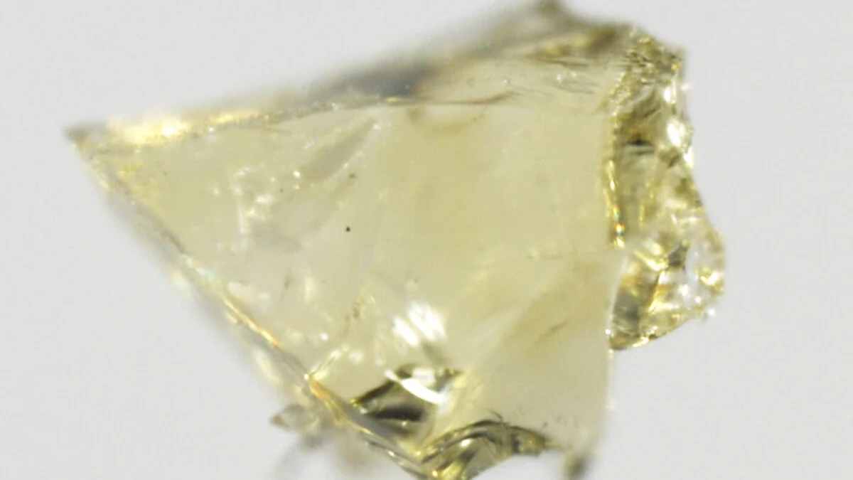
Some discoveries emerge from carefully designed experiments, while others begin with an unexpected observation that nobody intended to make. The story of Jan Czochralski belongs firmly in the second category. In 1916, while working with molten metal, the Polish metallurgist reportedly dipped his pen into the melt by mistake and noticed that a thin crystal filament formed as he pulled it away.The incident has become one of the most famous stories in materials science because it eventually led to the Czochralski method, a technique for growing large single crystals from molten materials. What began as an accidental observation later became a foundation of modern electronics.Today, the vast majority of silicon crystals used in semiconductor manufacturing are produced using variations of the process that carries Czochralski’s name, making his discovery one of the most influential laboratory accidents in industrial history.Jan Czochralski | Wikimedia CommonsA small mistake revealed an important processThe enduring appeal of the Czochralski story comes from its simplicity. According to accounts preserved by engineering institutions such as Northwestern University, the discovery occurred when Czochralski unintentionally introduced a pen into molten metal and observed a crystal thread forming as it was withdrawn.Whether described as molten tin or molten zinc, depending on the historical source, the key observation remains consistent. The metal did not simply cool randomly. Instead, it formed a structured crystal as it was pulled from the liquid. Many accidental observations are quickly forgotten, but Czochralski recognized that this phenomenon could be investigated systematically. His ability to pay attention to an unexpected result ultimately mattered more than the mistake itself.The method transformed crystal growthAfter the initial observation, the challenge became turning the phenomenon into a repeatable process. Materials science references describe the Czochralski method as a technique in which a seed crystal is brought into contact with a molten material and slowly pulled upward while carefully controlling conditions within the melt.The significance of this approach lies in its ability to produce large single crystals with highly ordered structures. In many industrial applications, especially electronics, crystal quality is critically important because imperfections can affect performance. By providing a reliable way to grow large crystals, the method opened possibilities that would have been difficult to achieve through less controlled techniques. This transition from accidental observation to reproducible process is what transformed the discovery into a major technological advance.Silicon gave the discovery global importanceThe invention’s influence expanded dramatically with the rise of the semiconductor industry. A major review published through PubMed notes that approximately 95 percent of the world’s silicon single crystals are produced using the Czochralski process.That figure highlights the extraordinary reach of the method. Silicon wafers serve as the foundation for microprocessors, memory devices, sensors, and countless other electronic components. Producing these wafers requires large, highly pure crystals, exactly the type of material the Czochralski method was designed to create. As electronics became central to modern life, the process moved from a specialized metallurgical technique to one of the most important manufacturing methods in the world.The technique continues to evolveOne reason the method remains influential is that it has proven adaptable to changing industrial demands. Contemporary research published in 2026 continues to examine process monitoring and temperature control during Czochralski silicon growth, demonstrating that the technique remains an active area of engineering development.This ongoing research reflects the increasing precision required by modern semiconductor manufacturing. While the basic principle remains similar to the one Czochralski observed more than a century ago, today’s production systems operate at scales and tolerances that early researchers could scarcely have imagined. The continued refinement of the process illustrates how enduring technologies often evolve rather than being replaced outright.Silicon crystal being grown by the Czochralski method at Raytheon, 1956 | Wikimedia CommonsAccidents only matter when someone investigates themThe popular version of the story sometimes creates the impression that luck alone produced the discovery. Historical evidence suggests a more interesting lesson. The accidental observation was only the beginning. The true breakthrough occurred because Czochralski studied what he had seen and transformed it into a systematic method.Many unexpected events occur in laboratories without leading to major advances. What distinguished this case was the decision to investigate rather than ignore the anomaly. Scientists and historians frequently point to this aspect of discovery because it demonstrates that curiosity and careful observation are often as important as planning. The accident provided an opportunity, but the method emerged through deliberate work and experimentation.Jan Czochralski’s observation of crystal formation in molten metal eventually became a reliable technique for producing the single crystals required by the semiconductor industry. More than a century later, the method continues to underpin silicon manufacturing and remains the dominant approach for producing many electronic materials. The story endures because it captures a truth that appears throughout the history of science: unexpected observations can change the world, but only when someone recognizes their significance and takes the time to understand them.
In 1916, a metallurgist accidentally dipped his pen into molten metal; it led to a crystal-growing technique that powers the modern semiconductor industry
In 1916, a Polish metallurgist inadvertently dipped his pen into molten metal, leading to a groundbreaking revelation. This serendipitous moment resulted in the formation of a crystal filament, which later became the Czochralski method—integral to modern electronics. This technique is now essential for producing most silicon crystals utilized in semiconductors, highlighting how a mere error can significantly impact industrial advancements.
TL;DRAI
A 1916 accident led Czochralski to discover a crystal-growth method now used for 95% of global silicon—critical to all semiconductor manufacturing. Continued temperature and precision refinements remain essential for competitive microprocessor and chip production.
810 words~4 min read