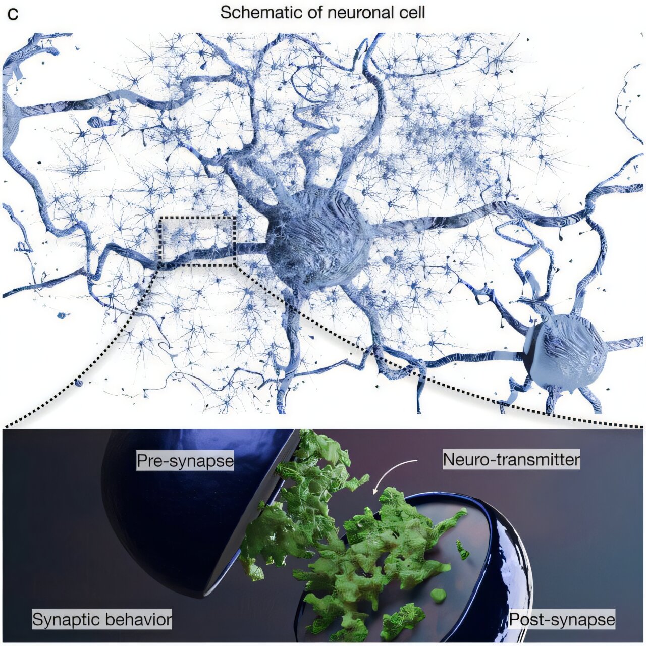
Schematic of a neuron and synapse, operating with transmission of the action potential. After initiation of the external stimulation, neurons transmit signal further to other neurons. Credit: Advanced Materials (2026). DOI: 10.1002/adma.73595
A research team led by Professor Taesung Kim of the School of Mechanical Engineering at Sungkyunkwan University (SKKU) has developed an optoelectronic synaptic device that mimics the functions of human neurons and synapses at the device scale. The researchers designed a van der Waals (vdW) crystal through a single-step sulfurization process using mixed plasma. The device operates under optical stimuli, offering a structural solution for configuring semiconductor materials for brain-inspired computing.
The findings were published in Advanced Materials.
Rapid advancements in artificial intelligence and hyper-connectivity require neuromorphic vision systems capable of sensing and processing vast amounts of visual data in real time. Optoelectronic synapses, which exhibit conductance variations in response to light signals, serve as core components of these systems.
Layered vdW materials have attracted significant attention as promising candidates because of their excellent optical properties and atomic-scale thickness. However, conventional vdW materials have faced technical challenges, including difficulty in precisely controlling grain boundaries and intercalation, polymer residue accumulation, mechanical warpage at interfaces, and poor large-area crystalline uniformity.