A silicon wafer is printed with intricate circuit designs, and shimmers with iridescent hues of pinks, blues, greens and yellows. Credit: Andrew Scott, OIST
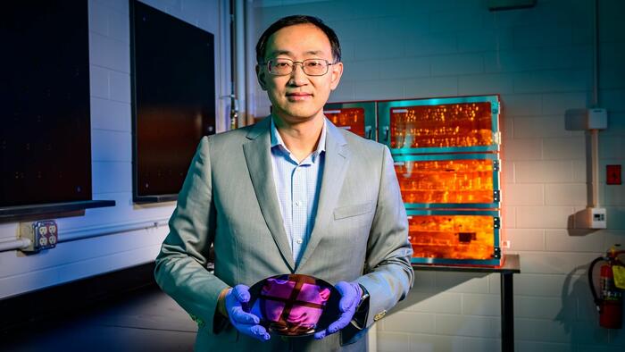
From data centers powering next-generation AI to vital medical technology, cars, and the mobile device or computer you're probably reading this on, semiconductor-based computer chips are essential to modern life.
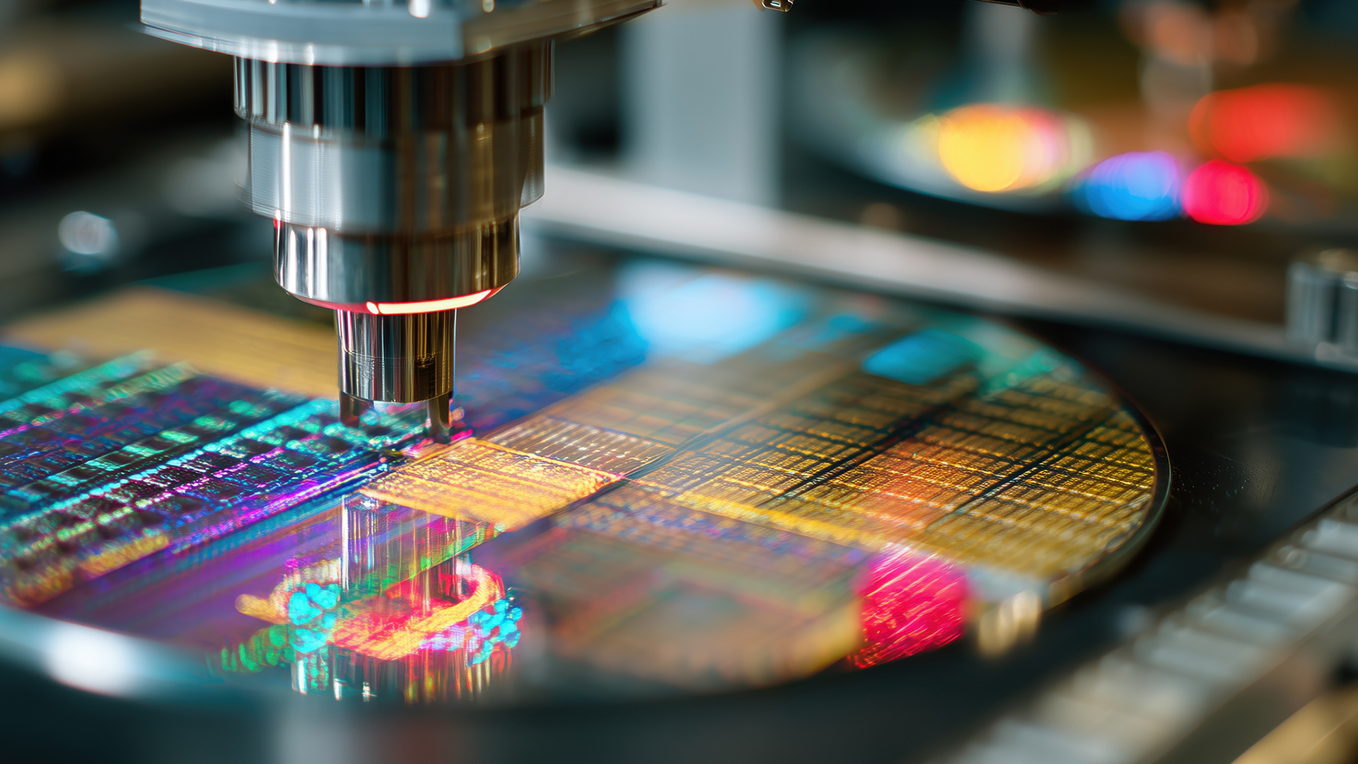
As technology advances and power consumption increases, scientists are hoping to create ever-smaller computer chips, requiring delicate chip designs on the individual nanometer (nm) scale. Methods such as extreme ultraviolet (EUV) lithography are providing new paths to these smaller chips, but they come with major physics, engineering and financial challenges, limiting current application and scalability.
Published in the Journal of Micro/Nanopatterning, Materials, and Metrology, Professor Tsumoru Shintake of the Okinawa Institute of Science and Technology (OIST) has proposed a radical redesign of the illumination systems and projectors used in high numerical aperture (high-NA) EUV lithography.
Simulations suggest that his design could eliminate troublesome optical (so-called "mask 3D") effects, enhance resolution and enable the manufacture of smaller computer chips at lower cost than current EUV methods.