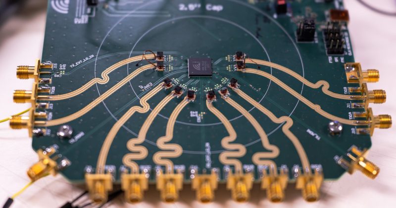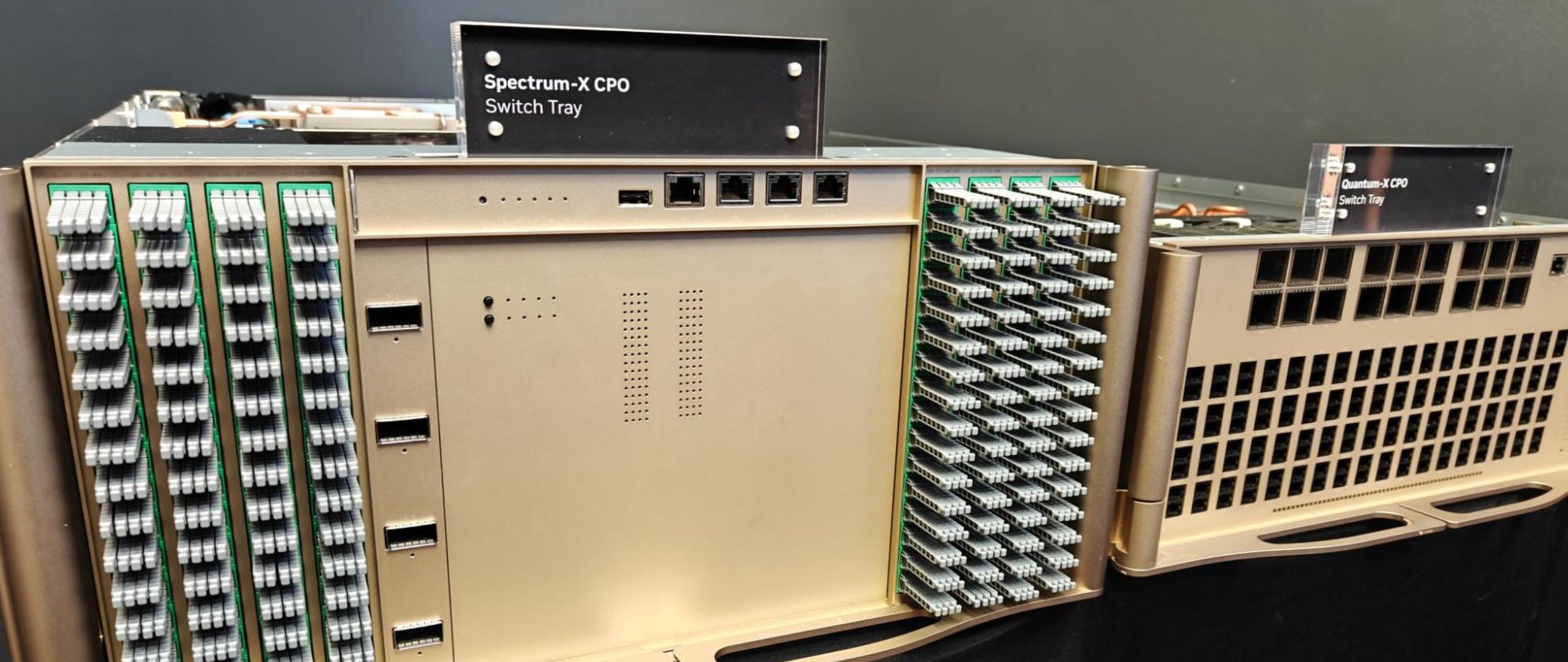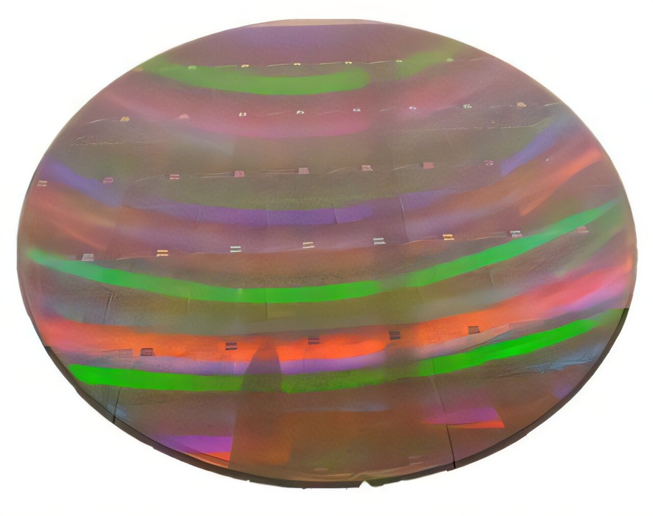
Micro-transfer printing enables highly flexible integration of two or more material systems in silicon photonics systems. Credit: Institute of Electrical and Electronics Engineers
The rapid growth of artificial intelligence and related computing infrastructure has exposed the limited bandwidth of conventional electrical interconnects in integrated circuits as a major bottleneck to system performance. Silicon photonics, which transmits data using photons instead of electrons, has emerged as a promising approach for overcoming bandwidth and latency limitations. The platform is now widely used for photonic integrated circuits (PICs), particularly in telecom and datacom applications.
A major strength of silicon photonics lies in its compatibility with standard complementary metal-oxide-semiconductor (CMOS) technology, enabling scalable PIC fabrication using existing semiconductor infrastructure. However, this also introduces a fundamental limitation. CMOS fabrication infrastructure is highly specialized and optimized and therefore cannot integrate nonstandard materials.
Conventional group-IV semiconductor materials cannot satisfy all requirements of advanced photonic systems, particularly for functions such as on-chip light generation. Materials such as III–V semiconductors and lithium niobate (LiNbO₃) can provide these capabilities, highlighting the need for heterogeneous integration approaches to expand the functionality of silicon photonics.