As AI workloads increase, explosive compute demand is pushing the semiconductor industry to meet unprecedented performance targets. Even small delays can have outsized financial impact in fast-moving AI hardware cycles. Simultaneously, the shift from chip-level optimization to system-level engineering is compounding thermal and power challenges.
Meeting these demands requires breakthroughs in materials deep within the device stack. This calls for advanced modeling and simulation beyond what conventional approaches can deliver.
This post explores how Applied Materials and NVIDIA are tackling this challenge with an end-to-end digital development model that combines Applied Materials leadership in materials engineering and semiconductor manufacturing with NVIDIA CUDA-X libraries. This collaboration accelerates the entire innovation pipeline—from atomic-scale discovery and engineering through process development to factory optimization.
How are NVIDIA and Applied Materials accelerating semiconductor innovation?
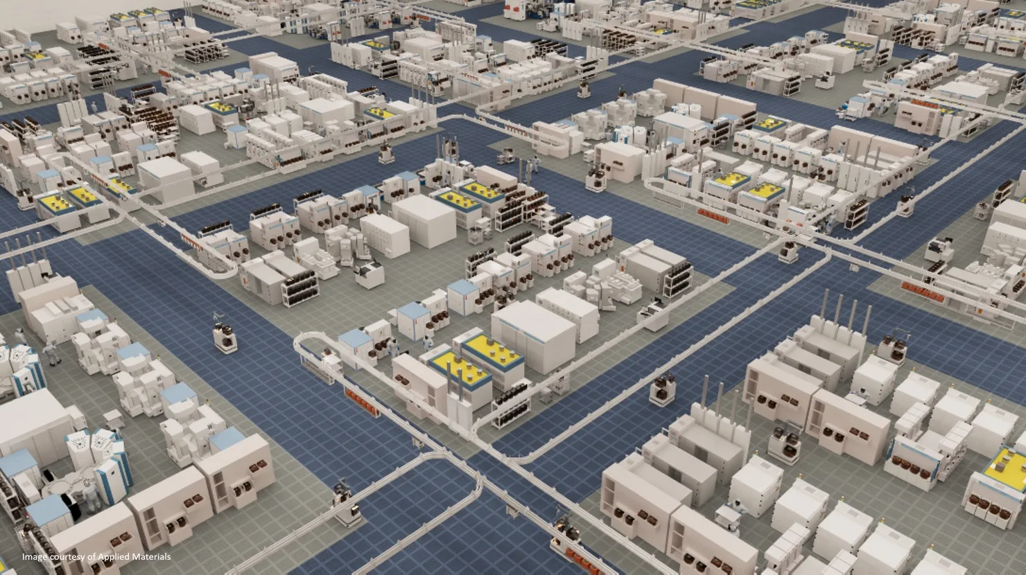
At the front end, GPU-accelerated simulations expand the design space, giving materials engineers a powerful advantage in developing next-generation devices. In the middle, physics-based modeling speeds up chamber and recipe development. At the back end, AI-driven digital twins predict fab performance before changes hit the production floor. Putting these together creates a continuous flow of insights that drives faster progress from atoms to fabs.