(Image credit: Getty Images)
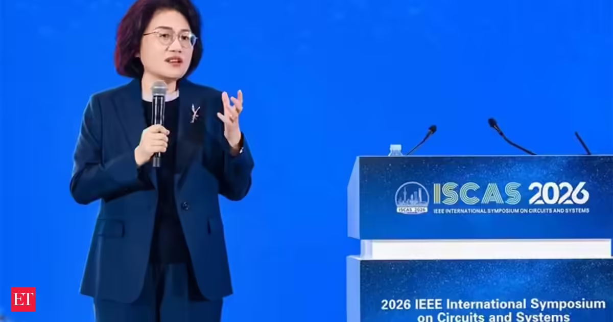
Peking University's School of Integrated Circuits has unveiled a prototype electronic design automation (EDA) tool built specifically for Huawei's LogicFolding architecture, according to the South China Morning Post. The tool takes what researchers described as a "true-3D" approach, optimizing an entire multilayer chip as a single vertical structure rather than designing each layer in two dimensions and stacking them afterward. In early tests of open-source circuit designs, the university reported a 30% reduction in total internal wire length, along with improvements in performance and thermal management, compared to conventional EDA workflows.The announcement came two days after Huawei presented LogicFolding and its accompanying Tau Scaling Law at the IEEE International Symposium on Circuits and Systems (ISCAS 2026) in Shanghai. Huawei's goal is to produce chips with transistor density equivalent to 1.4nm processes by 2031, all without access to the extreme ultraviolet (EUV) lithography equipment restricted under U.S. export controls.LogicFolding works by folding traditional 2D circuit layouts into vertical 3D stacks, shortening the physical paths that electrical signals travel through a chip. That reduces resistance and capacitance on critical wiring, compressing signal propagation delay. Huawei's Kirin smartphone processors launching later this year will be the first commercial chips to use the architecture.Go deeper with TH Premium: CPUSynopsys and Cadence both offer 3D IC design platforms for multi-die stacking and advanced packaging. But those tools address a different problem: integrating separate chiplets or dies within a package. LogicFolding folds transistor-level logic within a single chip into vertical layers, an intra-die optimization that requires place-and-route tools to work across the full vertical structure simultaneously instead of partitioning separate dies.Peking University's prototype reportedly addresses this by treating the multilayer structure as a unified design space from the start, but whether their claim of 30% wire-length improvement holds up at production scale remains to be seen.Synopsys, Cadence, and Siemens EDA command 31%, 30%, and 13% of the global EDA market, respectively, and their combined share within China exceeds 80%, according to EE Times China. The U.S. imposed and then lifted EDA export restrictions last year as part of a rare-earth materials deal. Still, the episode highlighted how dependent Chinese chipmakers remain on Western tools.China's domestic EDA companies, including Empyrean Technology and Primarius, have made progress in analog, mixed-signal, and physical verification, but none offer a full digital design flow competitive with the Western incumbents at advanced nodes.Get Tom's Hardware's best news and in-depth reviews, straight to your inbox.A university prototype is a very long way from production-grade commercial software. EDA tools require years of development, extensive process design kit integration with foundries, and validation across thousands of tape-outs before chipmakers trust them. "No single company can independently find all the answers along the path of semiconductor evolution," He Tingbo, chairwoman of the Huawei Scientist Committee and president of the company's semiconductor business department, said at a media briefing on Monday.