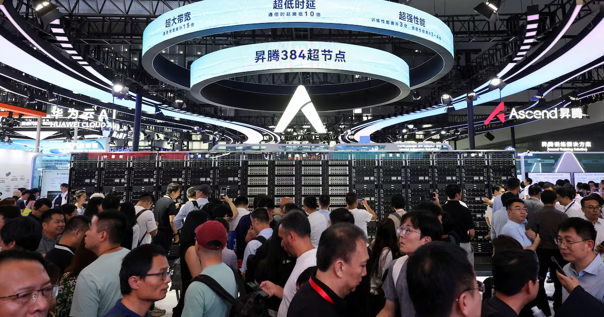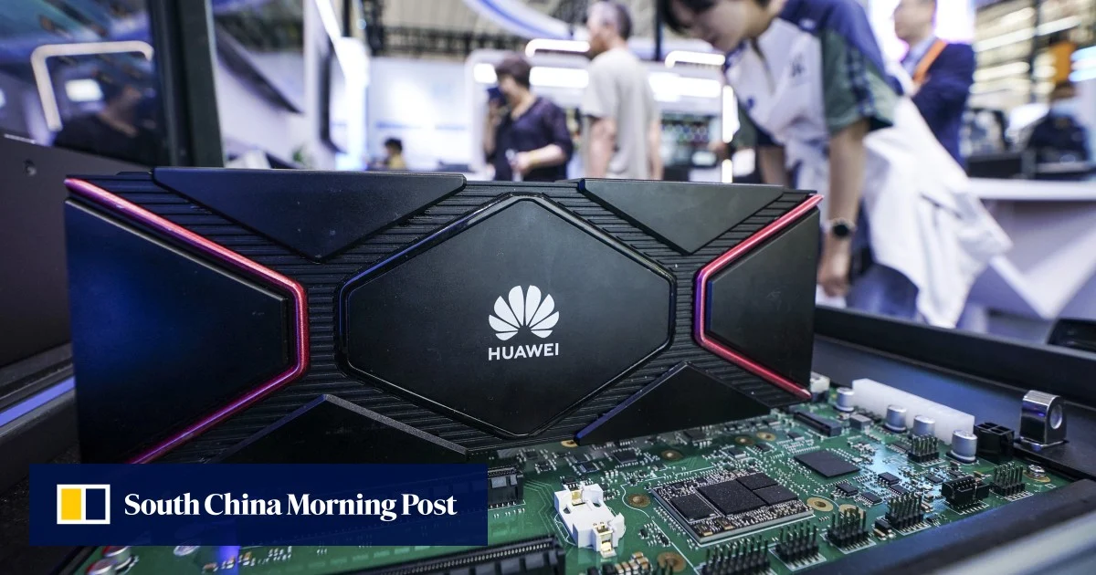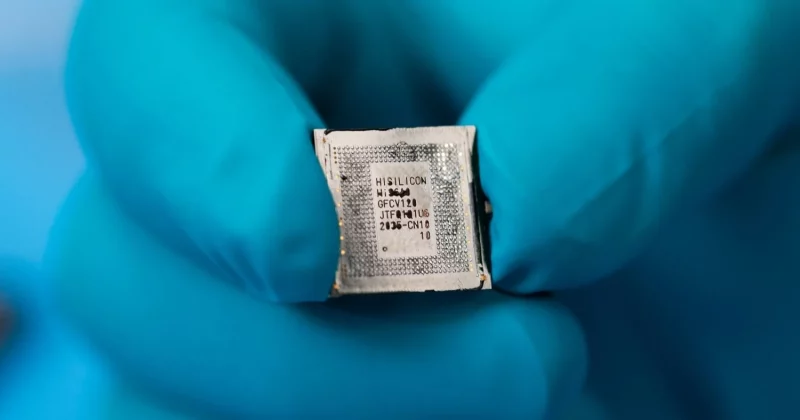
Huawei just told the world it found a workaround. And the market believed it.
Chinese semiconductor stocks surged in Hong Kong and Shanghai after Huawei unveiled what it calls a fundamental breakthrough in chip design, one that could let the company achieve performance on par with 1.4-nanometer processes by 2031, all without relying on the advanced lithography equipment that US sanctions have put out of reach.
What Huawei actually announced
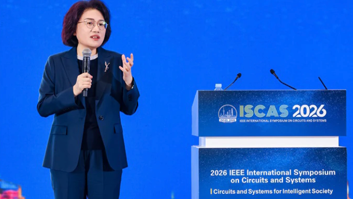
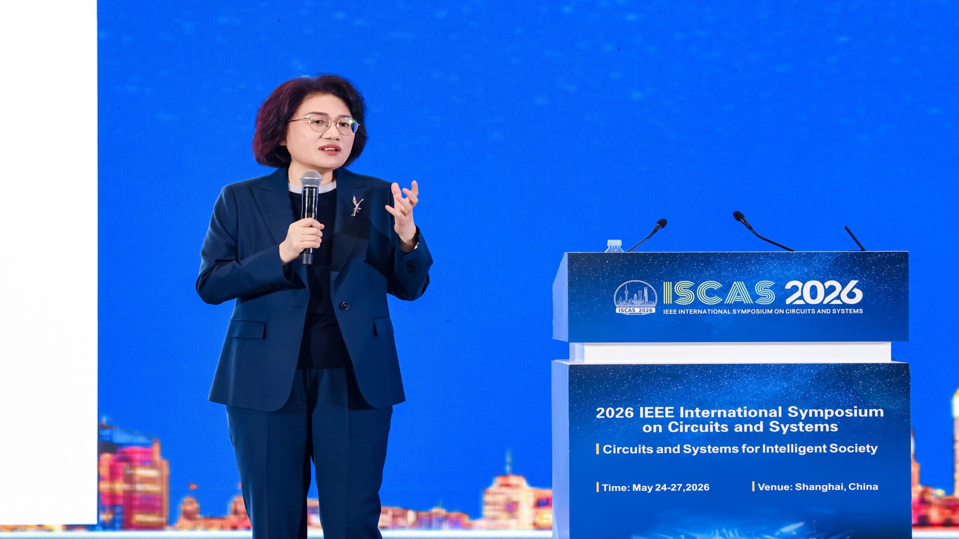
At an IEEE symposium in Shanghai on May 25, Huawei’s semiconductor president He Tingbo introduced two concepts: an architecture called “LogicFolding” and a principle dubbed the “Tau Scaling Law.” The core idea is that you don’t necessarily need to shrink transistors to make chips faster and more efficient. Instead, systemic optimizations across the entire chip design can deliver comparable gains.
The company says it has already mass-produced 381 chips based on the Tau Scaling Law over the past six years. That’s not a theoretical paper or a lab demo. That’s production silicon, if the numbers hold up.