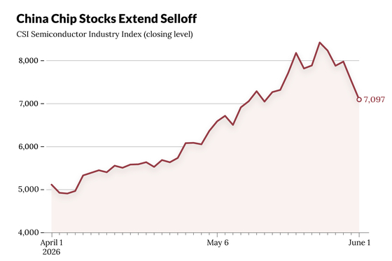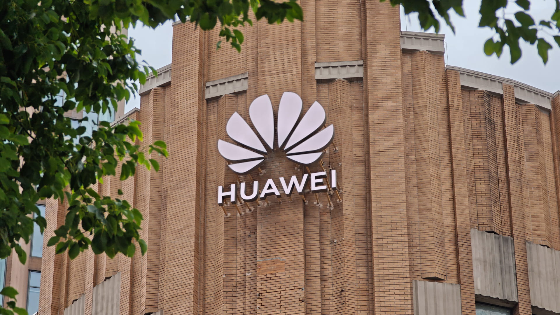
Huawei just told the world it plans to match 1.4-nanometer transistor density by 2031 without access to the cutting-edge equipment that makes those chips possible today. The market’s response was immediate and emphatic.
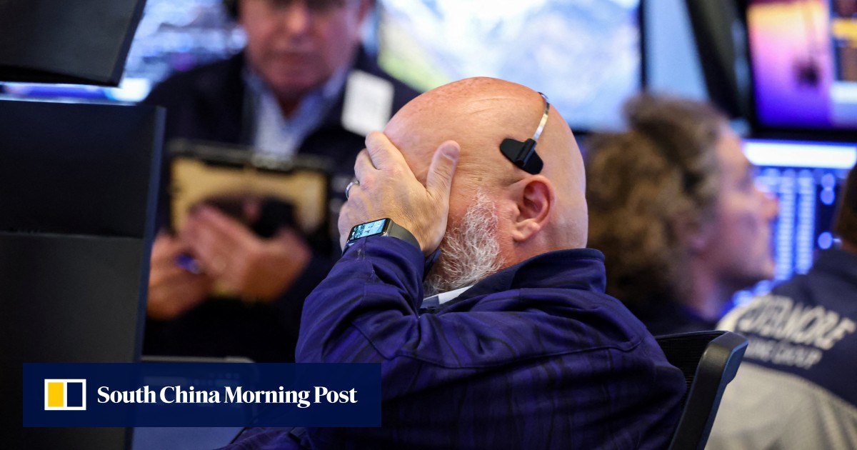
Shares of Semiconductor Manufacturing International Corporation (SMIC) surged more than 17% on May 26, while Hua Hong Semiconductor climbed over 16%. China’s broader semiconductor sector, valued at approximately $900 billion according to Bloomberg, is now riding a wave of optimism fueled by technological breakthroughs, upcoming IPOs, and the gravitational pull of artificial intelligence.
What Huawei actually announced
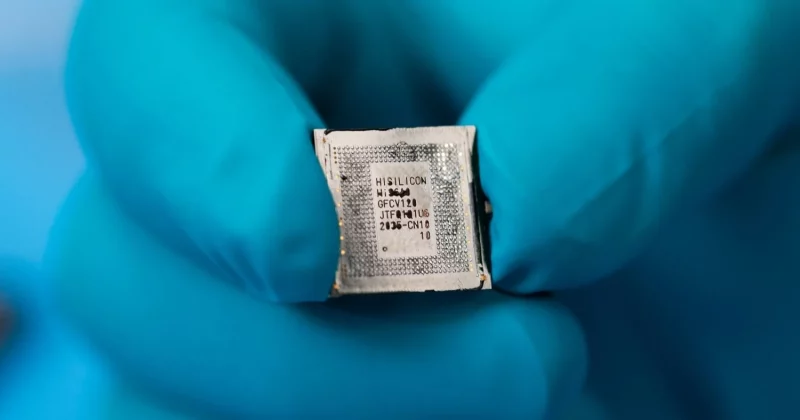
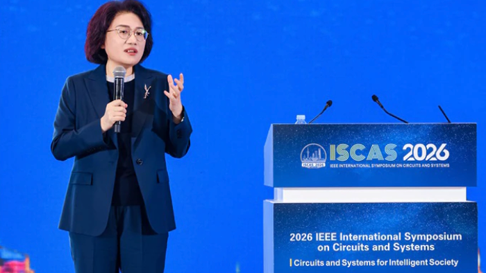
On May 25, Huawei’s semiconductor chief He Tingbo took the stage at the IEEE International Symposium on Circuits and Systems in Shanghai and unveiled two innovations: a chip design framework called “LogicFolding” and a theoretical scaling principle dubbed the “Tau Scaling Law.”
Traditional chip advancement has relied on making transistors physically smaller, a process that requires the most advanced lithography machines on the planet, machines China currently cannot buy due to US export controls. LogicFolding appears to take a different approach, achieving density improvements through architectural design rather than brute-force miniaturization.