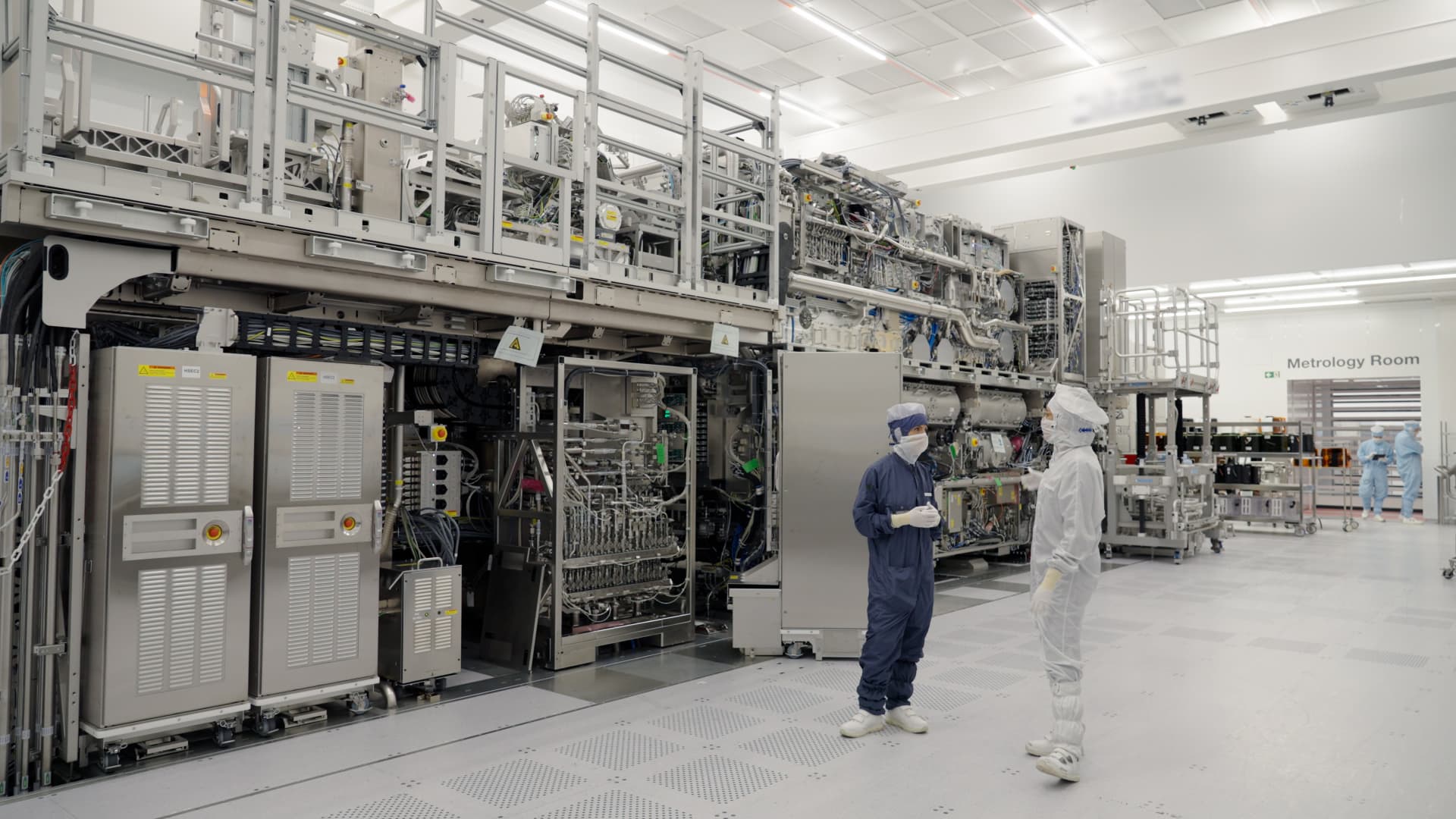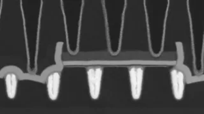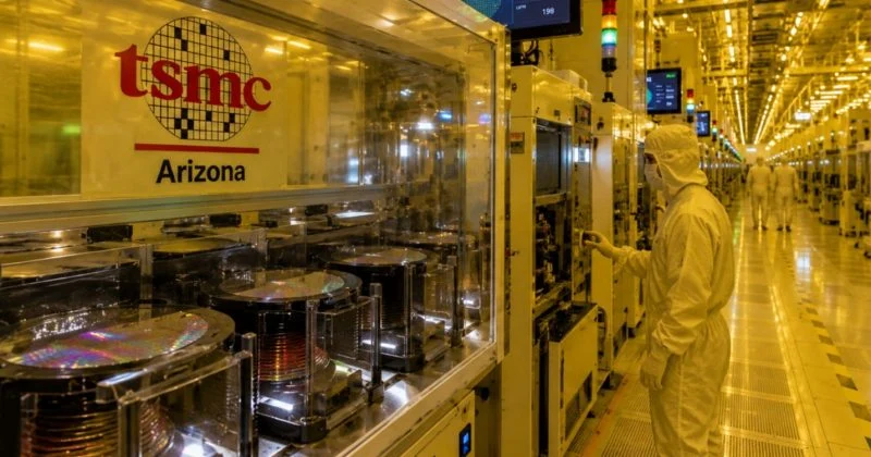
ASML, TSMC, and research institute imec have jointly demonstrated the first scaled complementary transistors built from 2D materials on standard manufacturing wafers, achieving a yield that makes commercial production look less like science fiction and more like an engineering timeline.
The results were presented in June 2026 at the IEEE/JSAP Symposium on VLSI Technology and Circuits.
What they actually built
The collaboration produced both n-type and p-type transistors at a contacted poly pitch of 50 nanometers. Contacted poly pitch (CPP) is essentially the repeating distance between transistor gates. Smaller CPP means you can pack more transistors into the same space, which is the whole point of Moore’s Law.
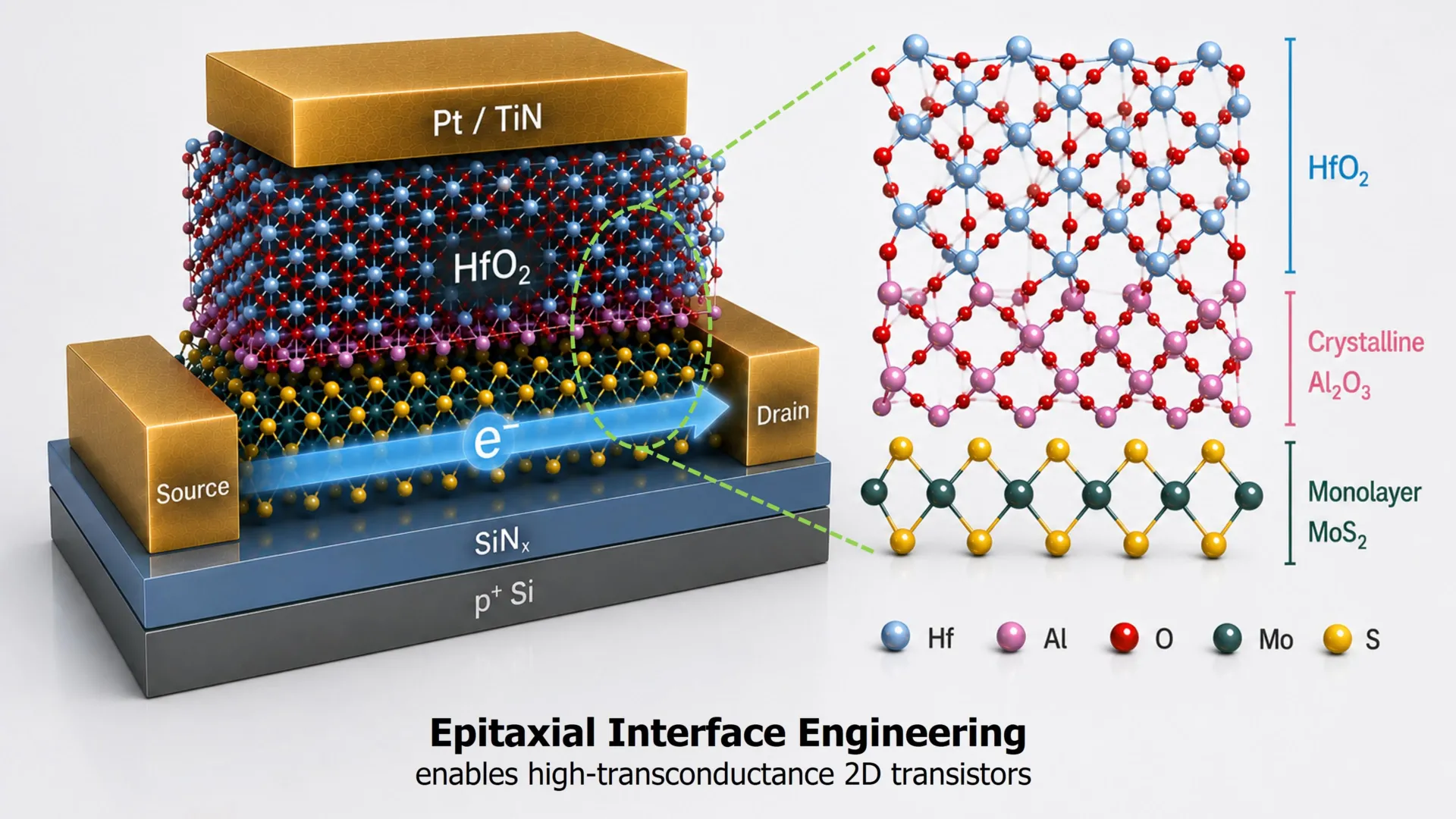
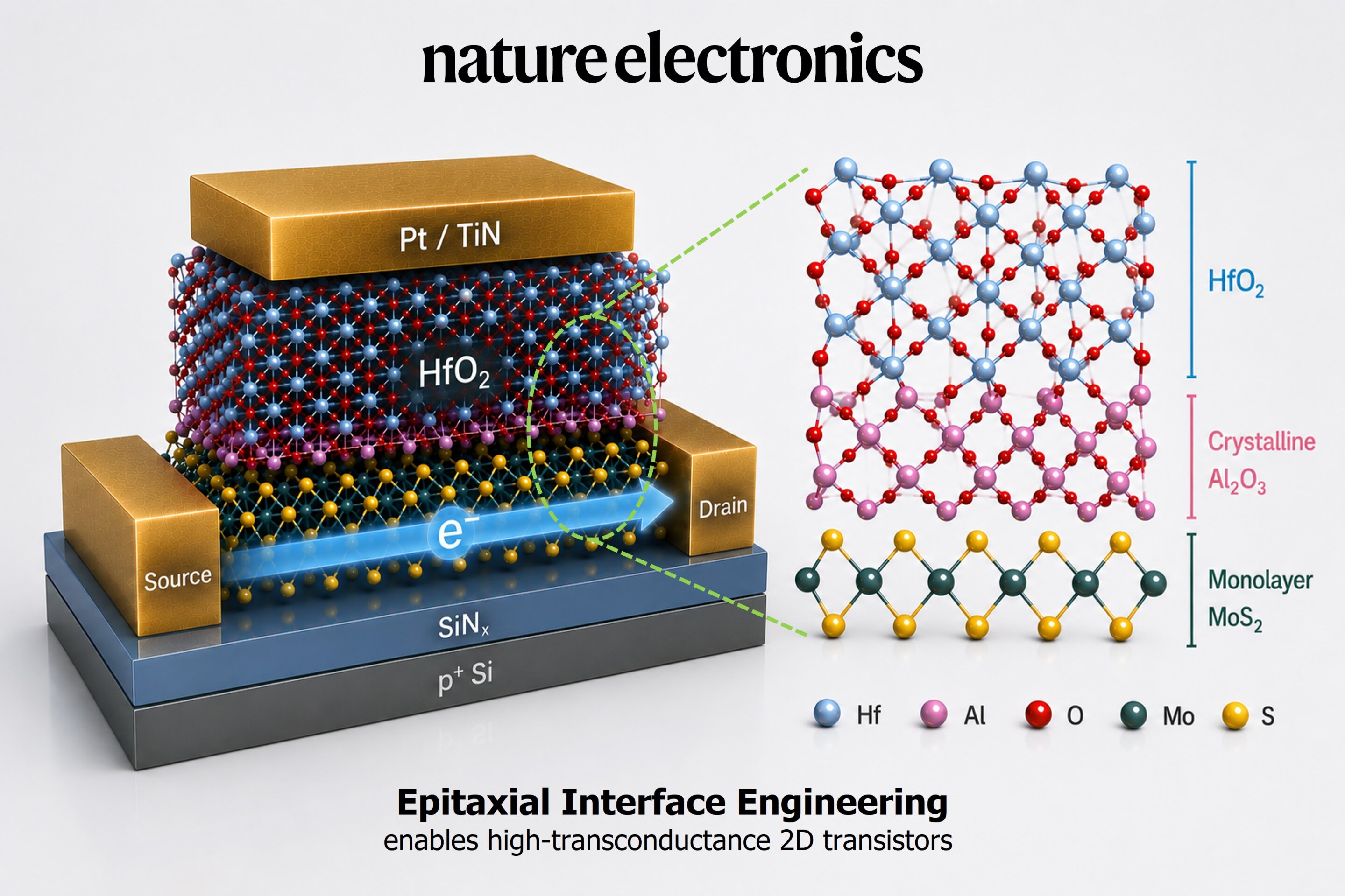
The n-type devices used molybdenum disulfide (MoS₂) as their channel material, while the p-type devices relied on tungsten disulfide (WS₂) or tungsten diselenide (WSe₂). These belong to a class of materials called transition metal dichalcogenides, which are atomically thin, two-dimensional crystals.