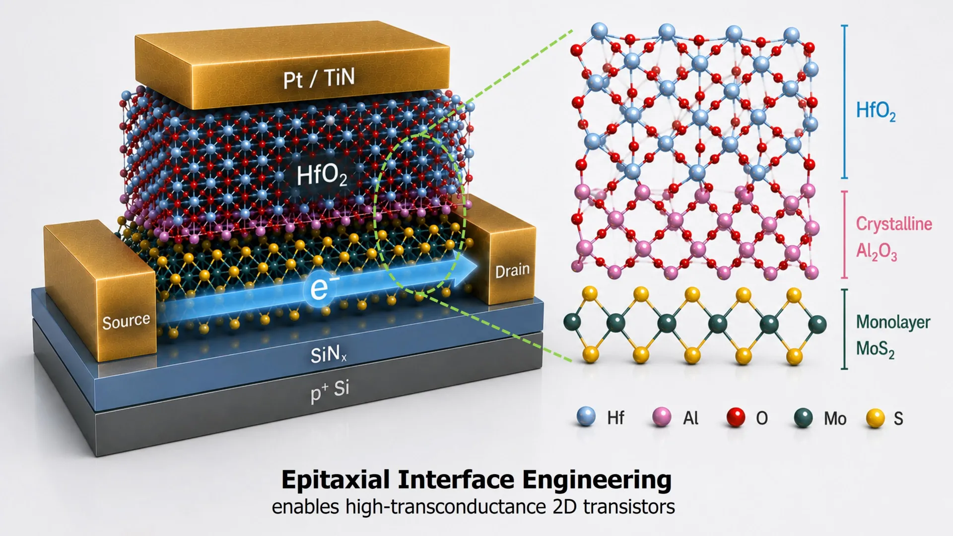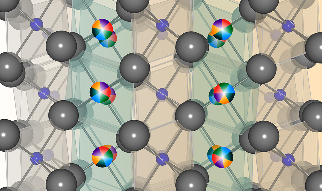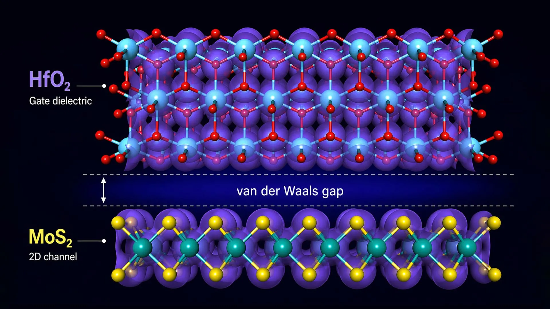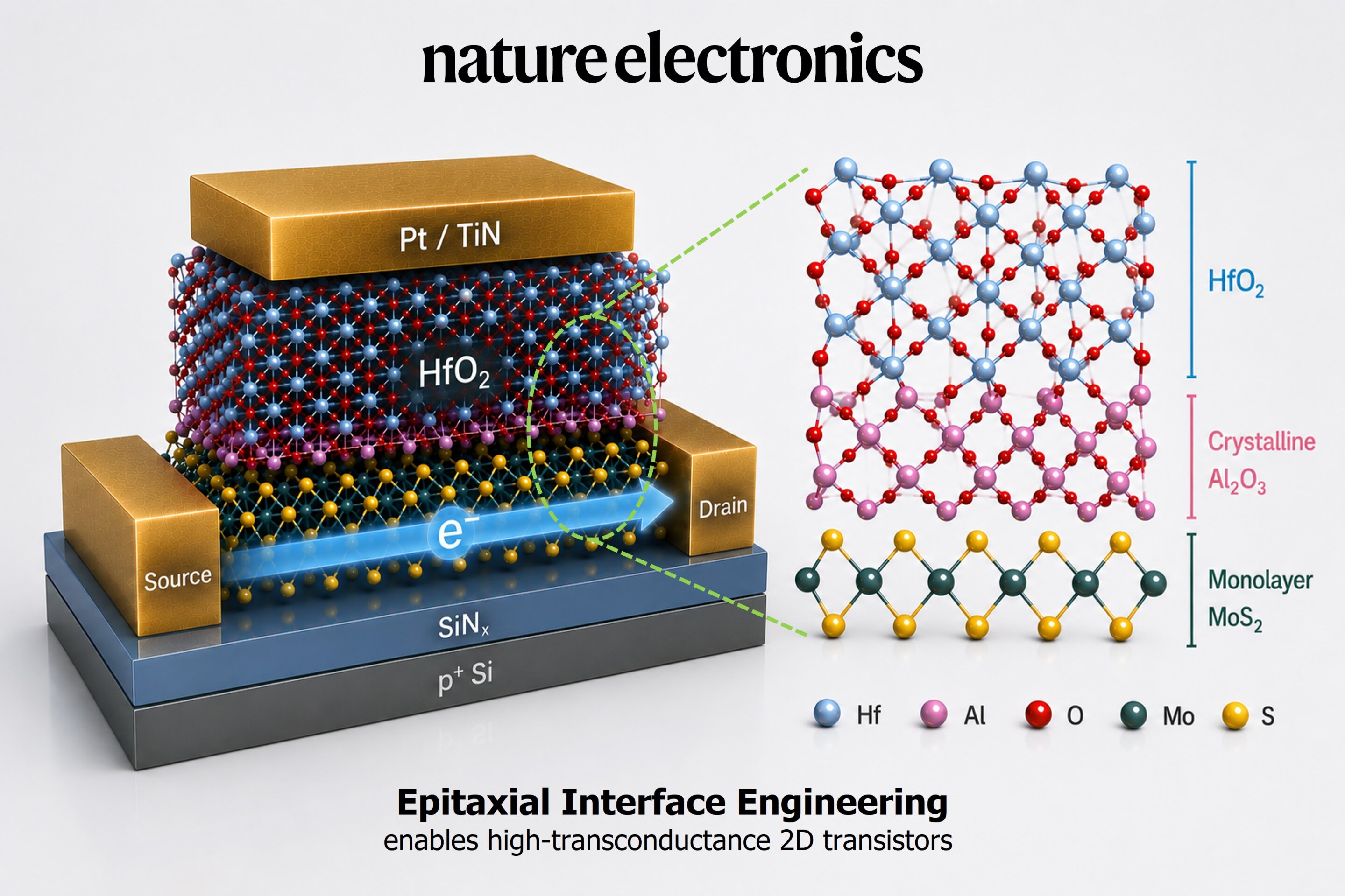
Researchers from NYCU and TSMC show that redefining the atomic boundary between materials can address a major engineering barrier restricting the development of next-generation semiconductor devices. Credit: Springer Nature
For more than 10 years, atomically thin semiconductors have been considered among the most promising alternatives to silicon. Only a single atom thick, these materials possess strong electrical characteristics and could facilitate the development of faster, smaller and more energy-efficient transistors that surpass the limits of current chip technology. However, despite significant advances in discovering new two-dimensional semiconductors, one persistent engineering obstacle continues to hinder progress.
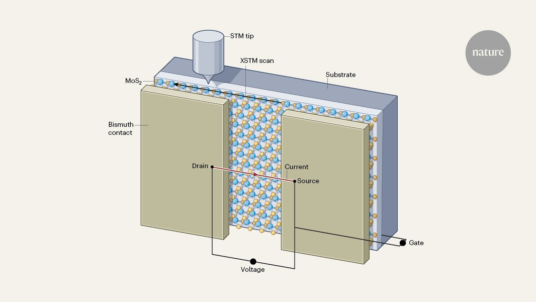
To create a functional transistor, engineers need to add an ultrathin insulating layer, called the gate dielectric, over the semiconductor to manage electron flow. Thinner layers enhance electrical control, which becomes crucial as transistors become smaller. However, using atomically thin materials can harm the sensitive electronic interface, causing electron scattering and impairing the performance improvements engineers aim for. For years, the semiconductor community has faced an uncomfortable compromise: improve gate control or preserve carrier mobility, but rarely both.