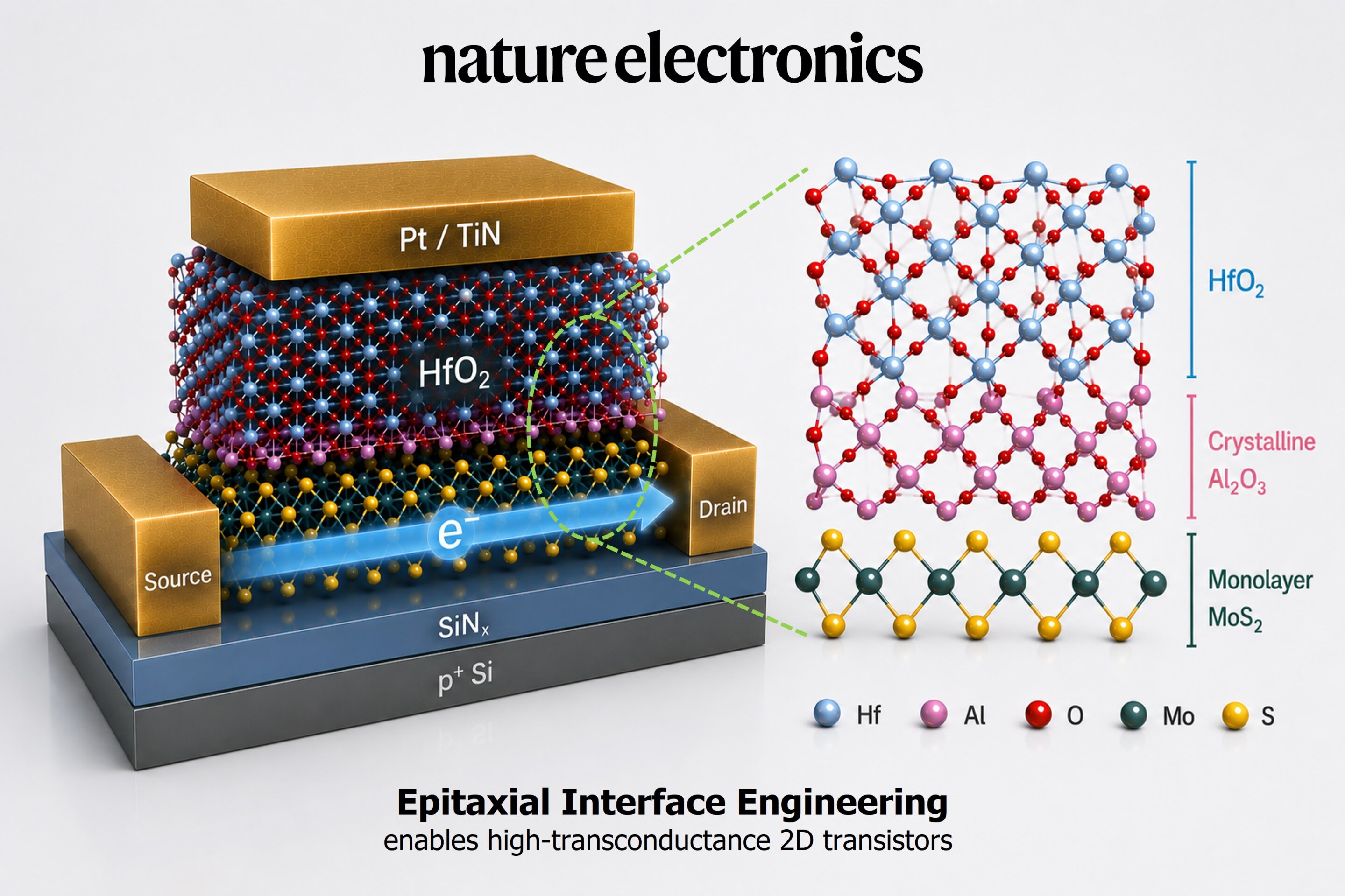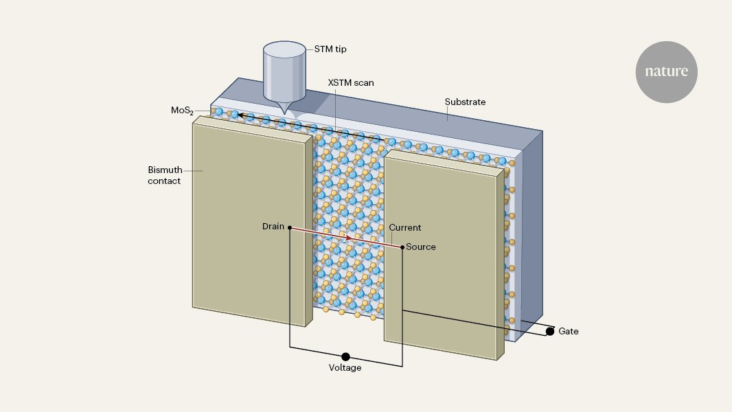
For more than a decade, atomically thin semiconductors have stood out as a promising route beyond conventional silicon. These materials can be just a single atom thick while still offering impressive electrical properties. In principle, they could enable transistors that are smaller, faster, and more energy efficient than today's devices. Yet even as researchers have discovered increasingly capable two-dimensional semiconductor materials, one stubborn engineering problem has remained.
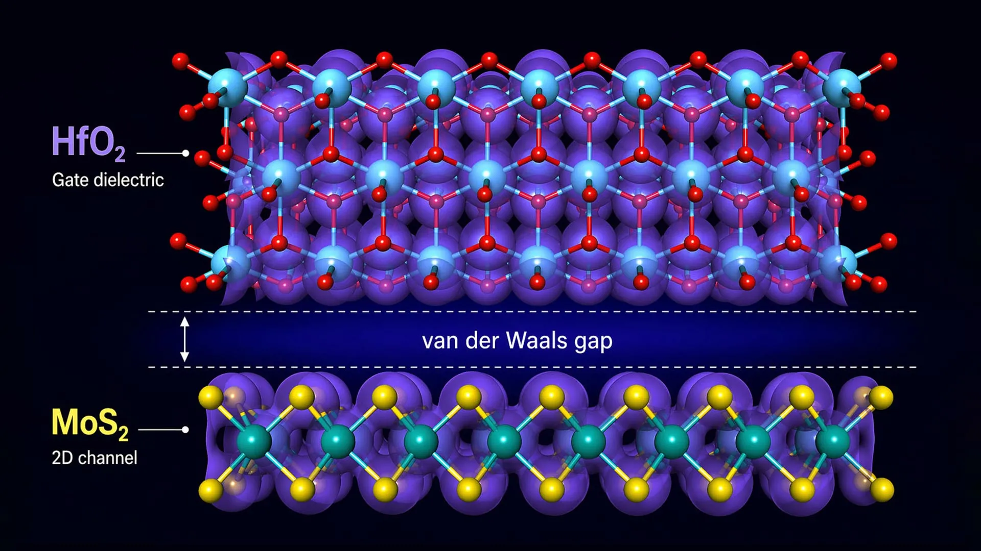
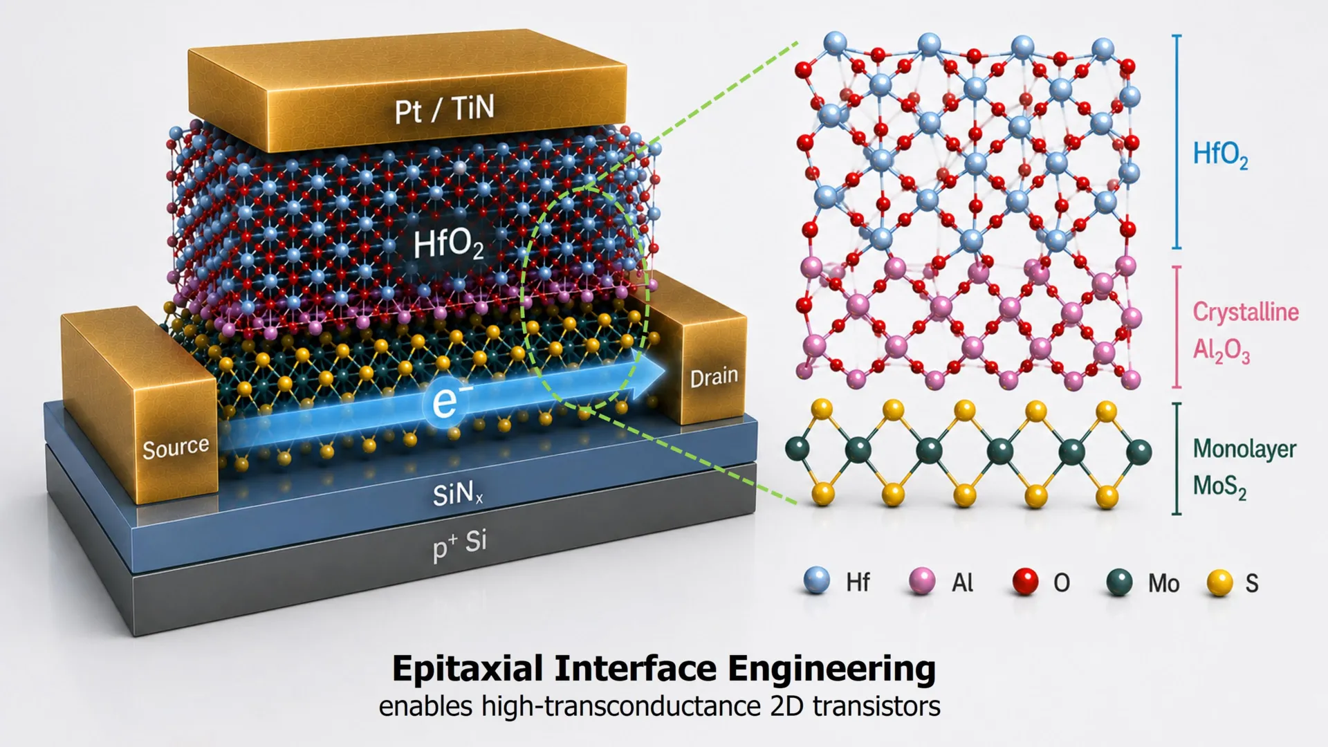
A working transistor requires an extremely thin insulating layer known as the gate dielectric. This layer sits above the semiconductor and helps control the movement of electrons. As transistors shrink, making this insulating layer thinner can improve electrical control. The difficulty is that adding such layers to atomically thin semiconductors can disturb the delicate interface between the materials. That disruption can scatter electrons and erase some of the performance gains engineers are trying to achieve.
For years, researchers have therefore faced a difficult tradeoff. They could strengthen control over the transistor gate, or they could protect the mobility of the charge carriers moving through the device. Achieving both at once has been much harder.