01 July 2026
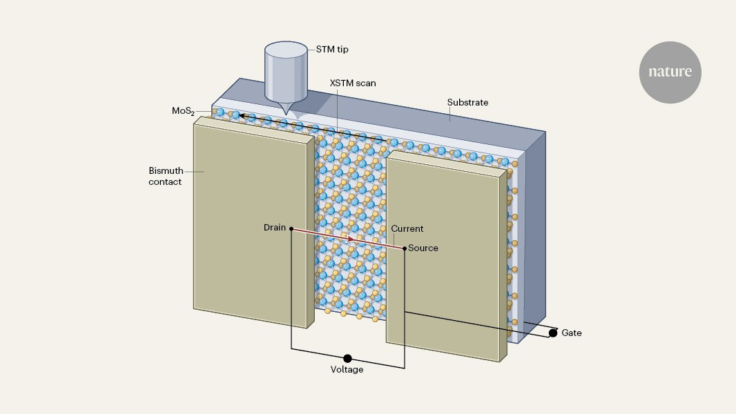
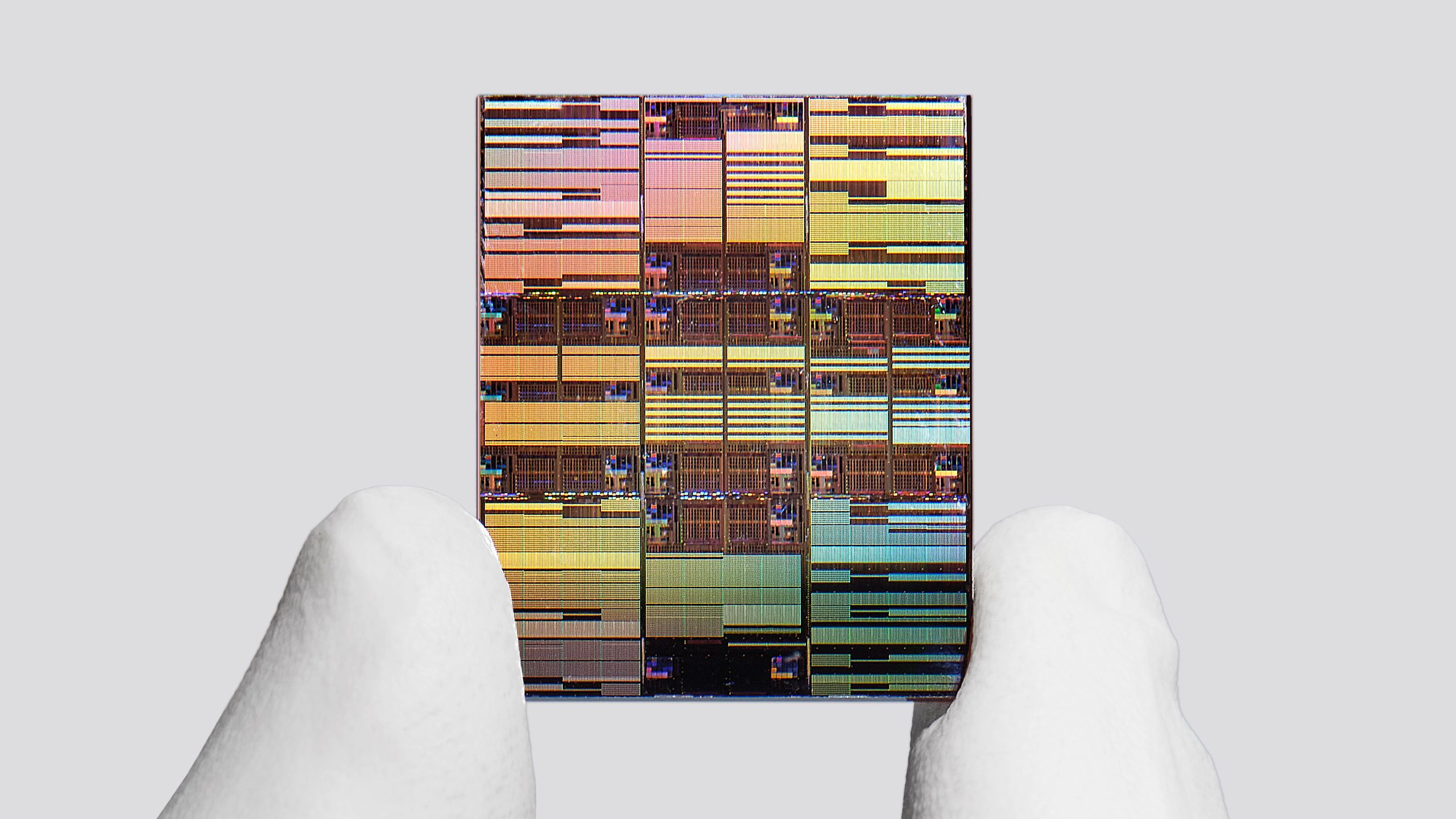
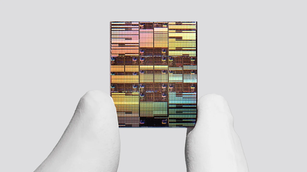
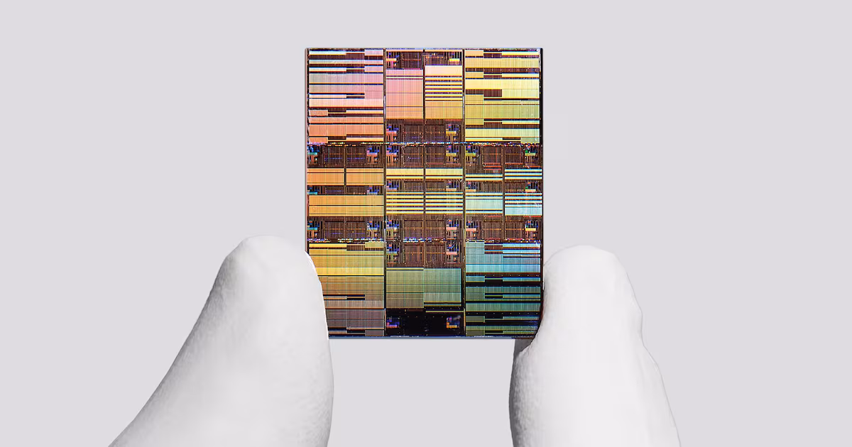
Direct imaging shows that the contacts through which current flows into atomically thin transistors can be scaled down to just a few nanometres in length.
By
Bent Weber0
Bent Weber
Direct imaging shows that the contacts through which current flows into atomically thin transistors can be scaled down to just a few nanometres in length.
01 July 2026
Direct imaging shows that the contacts through which current flows into atomically thin transistors can be scaled down to just a few nanometres in length.
By
Bent Weber0
Bent Weber

IBM unveils tech capable of producing chips smaller than one nanometre
0,7 Nanometer: IBM zeigt die ersten Chips mit CFET-Transistoren
Europäische Chipforschung: So stellt sich das Imec den Weg zu 0,2 Nanometern vor

IBM unveils sub-1-nanometer chip architecture that stacks 100 billion transistors onto a fingernail-sized processor
IBM mostra chip sotto 1 nanometro: la sfida ai limiti del silicio

IBM Unveils 3D-Stacked .7nm Chip Design | Silicon UK Tech News
IBM goes sub-1nm, develops 0.7nm-class technology — offering up to 50% higher performance and 70% higher energy efficiency compared to IBM's 2nm-class node
IBM Unveils Sub-1 Nanometer Chip With 100 Billion Transistors, Extending Moore's Law
IBM introduces 'first sub-1 nanometre chip' technology | The National
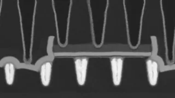
EUV-printed 28nm gates and 94% working devices, all on standard production tooling.

IBM has unveiled groundbreaking chip technology capable of producing transistors at 0.7 nanometers, a significant leap towards…

For more than 25 years, physicists have predicted that shrinking certain semiconductor nanotubes to extreme dimensions would…
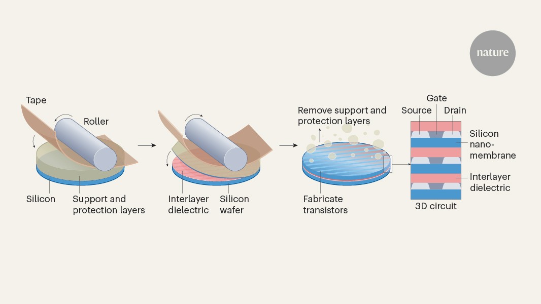
Stacks of transistors built from nanomembranes that can be rolled onto a substrate have been used to fabricate 3D circuits.
The global semiconductor market is approaching US$1 trillion in annual sales, driven by growing demand for faster computers,…

Inside computer chips are billions of tiny transistors made from silicon. But the material is approaching its limits. In an…