Serving tech enthusiasts for over 25 years.
TechSpot means tech analysis and advice you can trust.
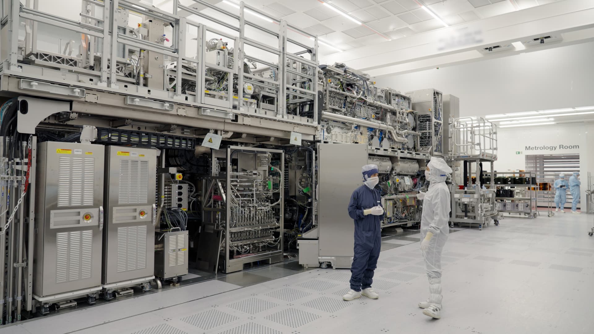
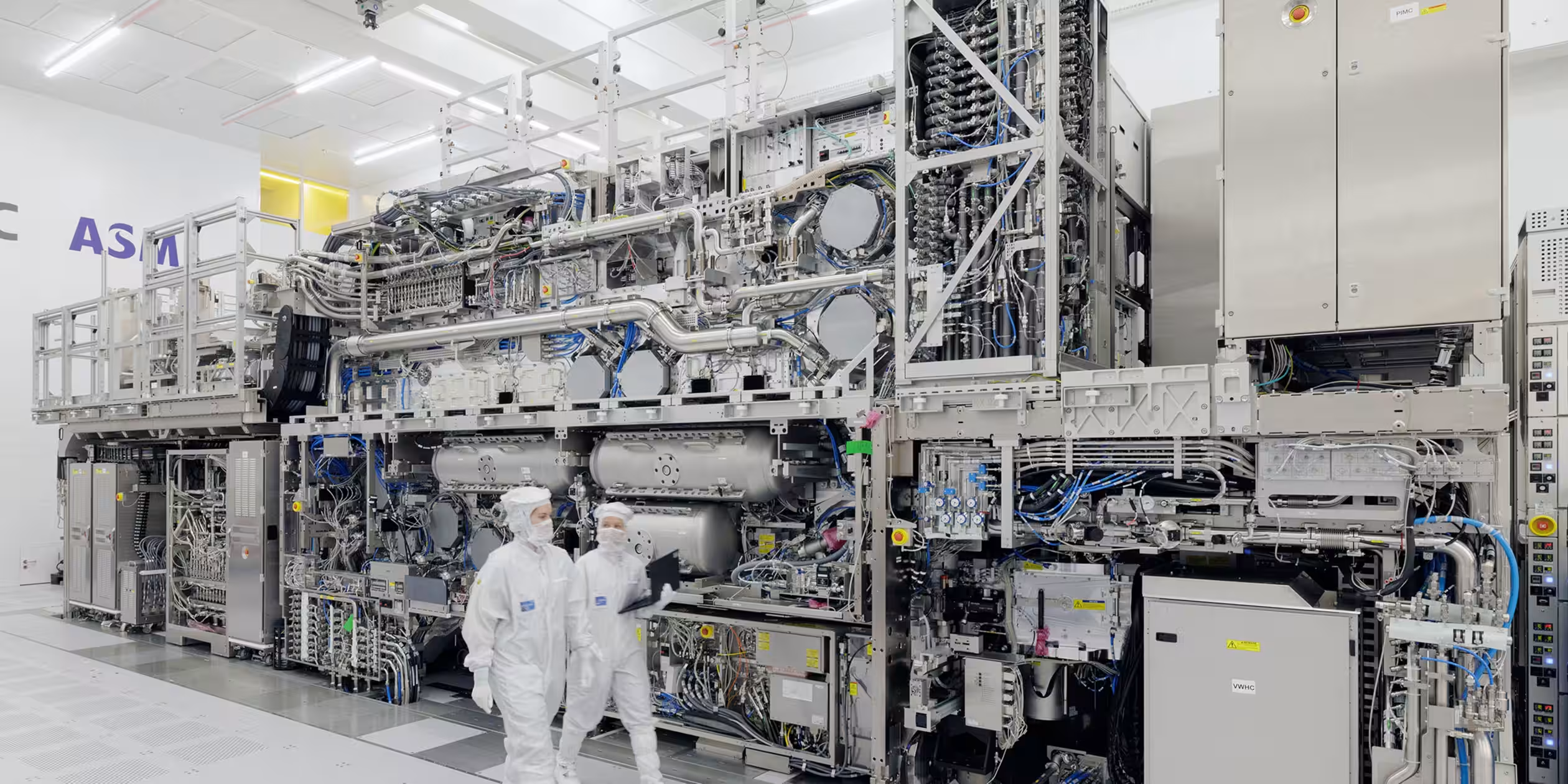
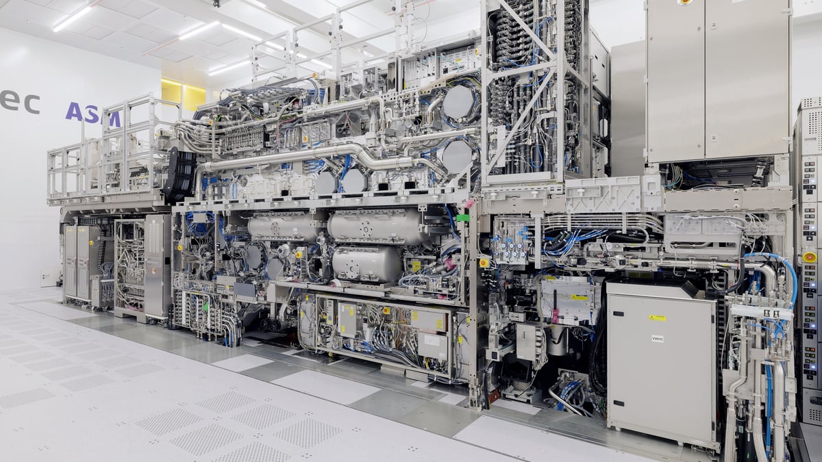
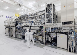
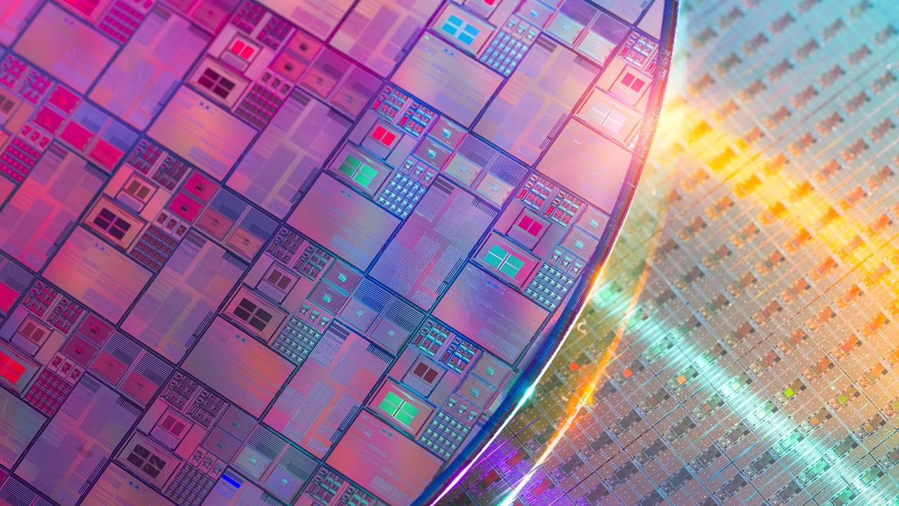
Forward-looking: ASML is working with customers on a larger mask format for its next-generation High-NA EUV lithography tools, a change that could make the systems more useful for the biggest AI and data center chips. The company's current EUV machines can print chips measuring up to about 800 square millimeters. That's large enough for processors and accelerators designed by Nvidia, Google, and other companies building advanced data center hardware.
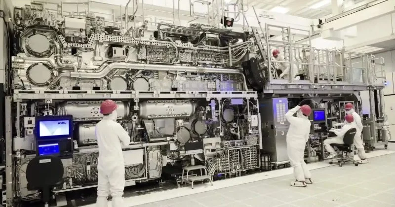
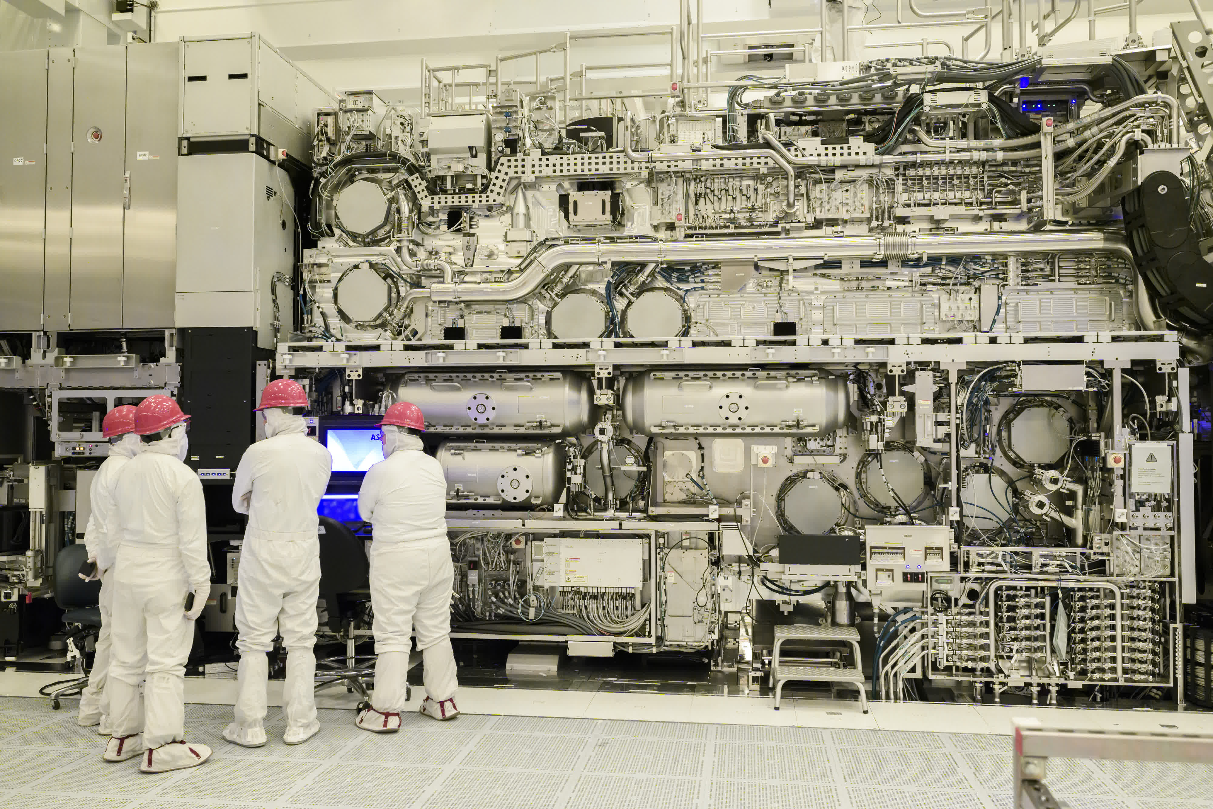
High-NA EUV is ASML's next major lithography platform. It can print finer features than today's EUV tools, which could help chipmakers build denser designs at advanced nodes. But its smaller mask limits the die area that can be printed in one exposure.
ASML now plans to move to a 12-inch mask format for High-NA EUV. The larger mask would allow the new machines to handle chips as large as the biggest data center devices made with existing EUV equipment.