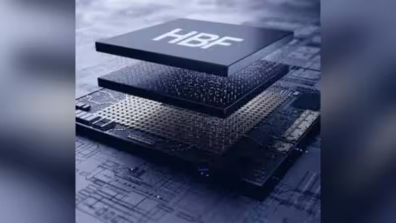
SanDisk just finished designing its first High Bandwidth Flash memory die, a milestone that puts the company on track to deliver product samples in 2027.
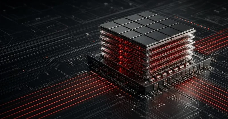
High Bandwidth Flash, or HBF, is SanDisk’s bet that you can take existing NAND flash technology, stack it in clever ways, and get performance that comes remarkably close to the pricier High Bandwidth Memory chips currently dominating AI hardware. Close as in within 2.2% of theoretical HBM limits, according to SanDisk’s projections.
What HBF actually does
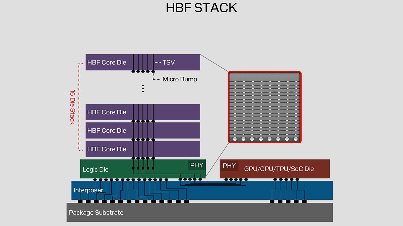
The first generation targets up to 512 GB per stack with read bandwidths around 1.6 TB/s. For context, that capacity figure represents roughly 8 to 16 times what existing HBM systems can offer in comparable configurations. Future iterations on the roadmap push performance to 2 TB/s and eventually 3.2 TB/s.
SanDisk plans to offer initial HBF configurations in 8-high and 16-high stacks, with bandwidth grades spanning from 0.4 TB/s to 3 TB/s depending on the configuration. The technology leans on SanDisk’s proprietary CBA and BiCS NAND processes, both of which the company has been refining for years in its conventional flash business.