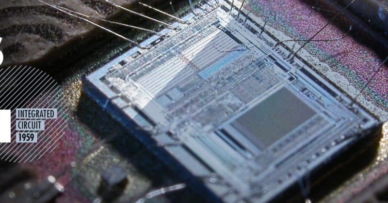
Applied Materials unveils more advanced chipmaking gear for 3D stacking architectures
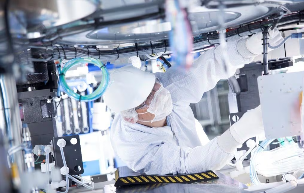
Chipmaking equipment giant Applied Materials Inc. is trying to make life easier for its chip fabrication plant customers, so they can build the extremely complex 3D architectures necessary for the next generation of artificial intelligence processors.
To do this, it has unveiled a host of new chip fabrication systems that span advanced packaging, process control and dynamic-random access memory manufacturing. The new machinery will help semiconductor manufacturers to increase their production volumes and yields for more sophisticated, powerful and energy efficient chips, which stretch their existing manufacturing capabilities to the limit.
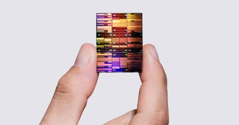
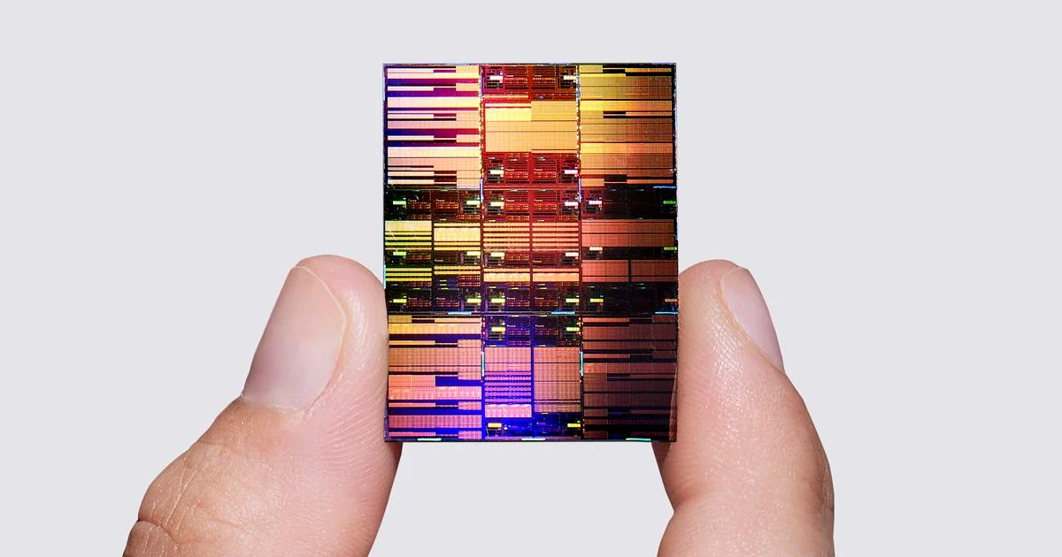
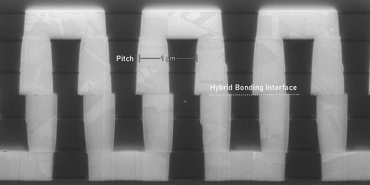
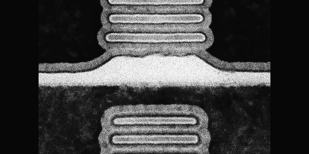
Applied Materials is trying to help chip companies overcome what’s known in AI infrastructure circles as the “memory wall.” As AI models become more powerful and capable, existing silicon processors can no longer keep pace with their extreme memory and bandwidth demands. To overcome this challenge, most chipmakers have gravitated toward more advanced packaging architectures that involve 3D stacking techniques and the use of high-bandwidth memory components.
But 3D stacking is extremely complex. The process requires multiple DRAM chips to be stacked on top of one another and connected using microscopic through-silicon vias or TSVs. It can dramatically increase the data throughput of processors, but manufacturing these chips is an extremely intricate process. Add in the problem of shrinking dimensions, uneven interconnects and the physical fragility of these ultra-thin processors, and it becomes almost impossible to manufacture them without high defect rates that eat away at production yields.