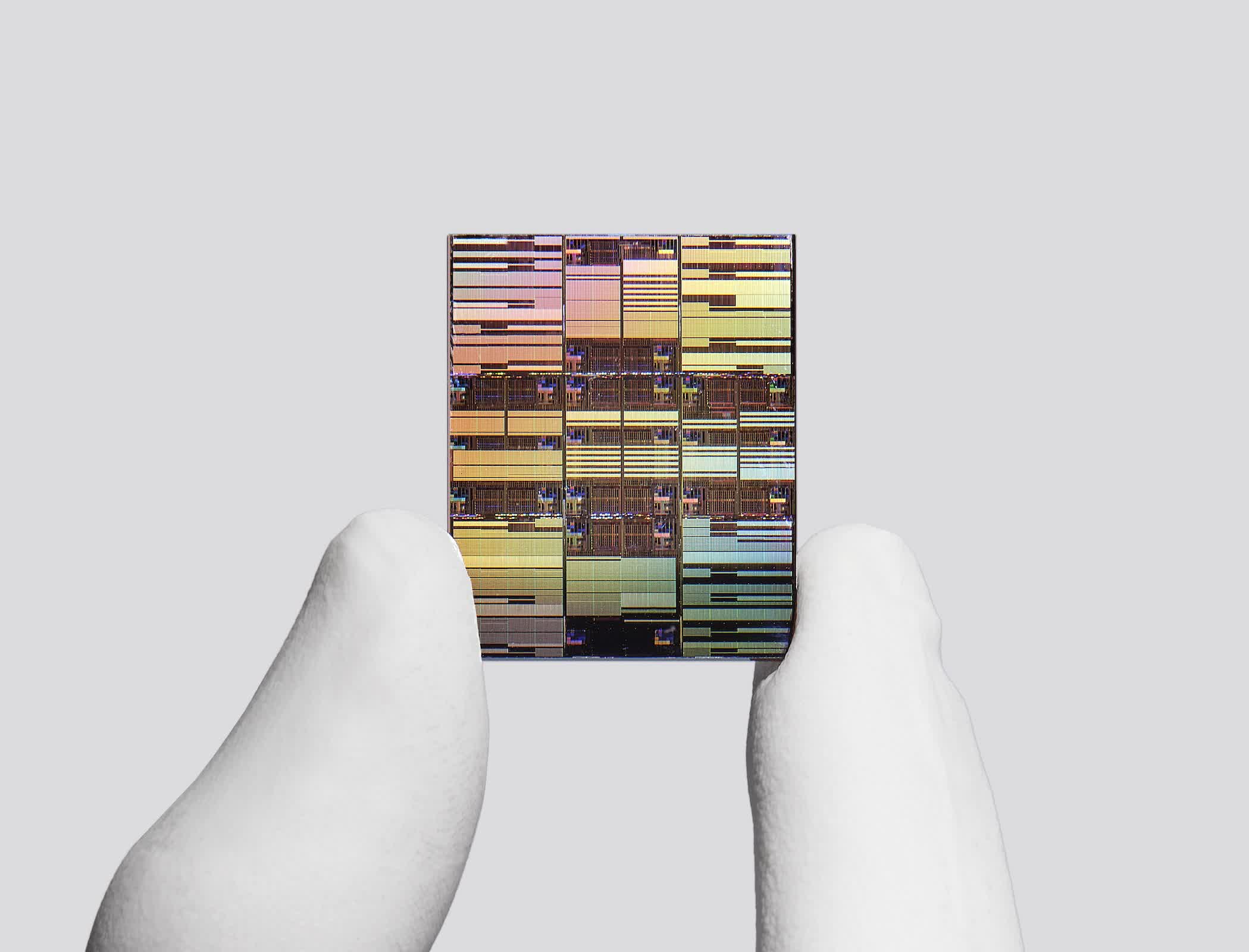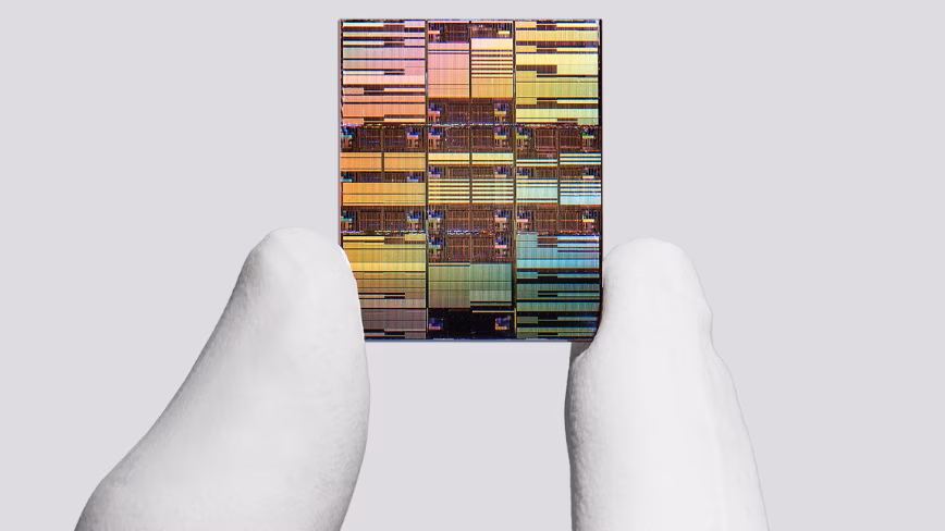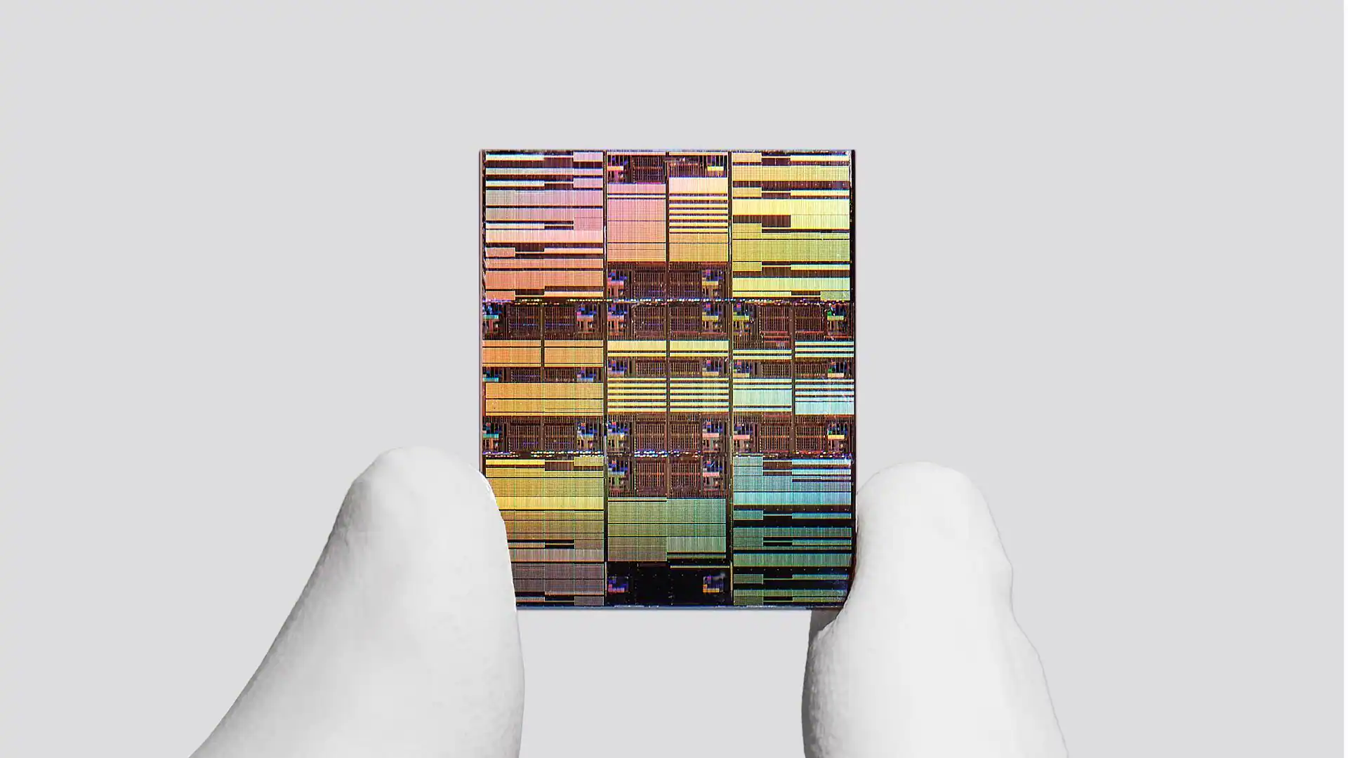
Researchers at the University of Illinois Grainger College of Engineering, working alongside IBM and other chip giants, have published a new method for vertically stacking transistor layers using ultrathin silicon nanomembranes. The results, published in Nature on May 30, 2026, show device yields of 98-100%, a number that makes the technique commercially viable rather than just academically interesting.
How vertical stacking changes the game
Traditional attempts at 3D chip integration have been hamstrung by heat. Previous methods required temperatures around 400 degrees Celsius, which tended to damage the lower layers of circuitry already in place.
The Illinois team solved this by using junctionless transistors built on silicon nanomembranes just 10 nanometers thick. Their process works at temperatures of 200 degrees Celsius or below, which keeps existing layers intact.
The researchers demonstrated three stacked layers, each containing 625 transistors, achieving current densities on par with conventional bulk silicon devices.