Insider Brief
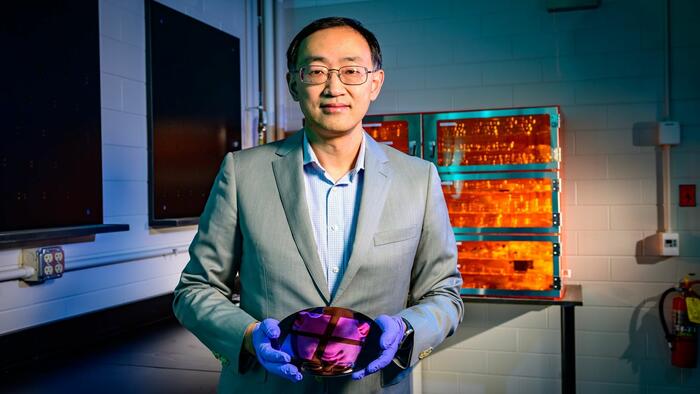
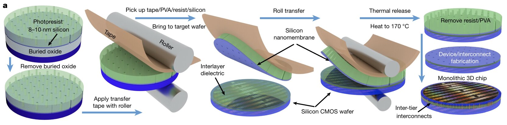
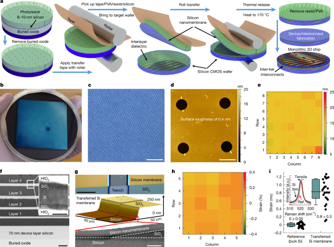
Researchers at the University of Illinois developed a low-temperature process for sequentially stacking silicon transistor layers, enabling monolithic 3D chip integration while remaining within industry thermal limits.
The team demonstrated three vertically stacked silicon layers containing 625 transistors each, achieving device yields of 98–100% and performance comparable to conventional silicon devices.
The approach is designed to support continued increases in computing density and efficiency by extending chip scaling beyond the limits of traditional transistor miniaturization.
The research, accompanying images, and supporting materials were provided by the University of Illinois Grainger College of Engineering.