FORWARD-LOOKING: For years, the chip industry has chased better performance by shrinking transistors and squeezing more of them onto a flat slice of silicon. That strategy is running into hard limits. A group at the University of Illinois thinks the next gains will come not from going smaller, but from going vertical.
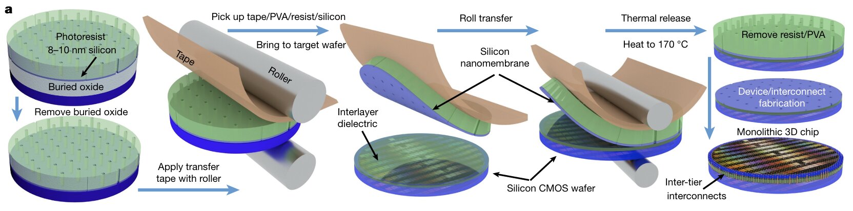
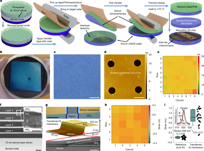
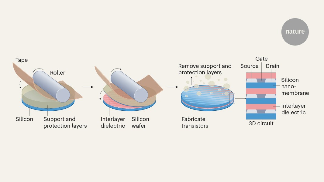
At the Grainger College of Engineering, materials science and engineering professor Qing Cao and his team have built working silicon circuits by stacking active layers directly on top of each other. Instead of adding more devices side by side, they are moving into the third dimension and building stacked layers on a single chip.
The push comes at a moment when traditional scaling is slowing. For roughly six decades, Moore's law has described an industry cadence where transistor counts and performance rise on a predictable schedule as features shrink. Now, that roadmap is harder to follow.
"In a sense, we're hitting a limit imposed by physics," Cao said. "If you look at the actual size of transistors, they're not getting smaller, especially in terms of their contacted gate pitch. This is because we're becoming limited by the intrinsic material properties of silicon and the fundamental rules of quantum mechanics."